Posts

[IFA 2022] LG Electronics Micro LED TV, QNED 8K TV(MiniLED)

#ifa2022 #lg #ledtv

▶ UBI Research website
https://ubiresearch.com/en/

▶If you are curious about the latest news related to OLED?
https://en.olednet.com/

▶Business, display report inquiry
marketing@ubiresearch.com
+82-2-577-4391

Analysis of 65-inch Premium TV Price Trends in the First Quarter of 2022

We analyzed the prices of 65-inch TVs of Samsung Electronics’ QLED TVs, OLED TVs from LG Electronics and Sony, and LG Electronics’ QNED TVs until March 2022.

The models we investigated at Samsung Electronics were 4K high-end model QN90A, 4K entry-level models QN85A and QN80A, and 8K models QN800A and QN900A. The models at LG Electronics were OLED TVs A1, C1, and G1 models and QNED TVs QN90UP and QN99UP. The models at Sony Electronics were OLED TV XR65A80J and XR65A90J.

The prices of Samsung Electronics’ 4K models QN90A, QN85A, and QN80A were $2600, $2200, $1700, respectively and the 8K models QN900A and QN800A were $5000 and $3500, respectively. The launch prices of LG Electronics’ OLED TVs A1, C1, and G1 were $2000, $2300, and $3000, respectively while the QNED TVs QNED90UP and QNED99UP were $1600 and $2700, respectively. Sony’s OLED TVs XR65A80J and XR65A90J were priced at $2800 and $4000, respectively.


As of March, the highest-priced 65-inch premium TV model was Sony’s XR65A90J. The lowest-priced model was Samsung Electronics’ QN65QN80A.

The prices of most of Samsung Electronics’ products have been falling since December. As of March, Samsung Electronics’ 80A, 85A, and 90A models are priced at $150, $200, and $500 lower than LG Electronics’ A1, C1, and G1 models, respectively, to induce consumption.

The price of LG Electronics’ OLED A1 and G1 models did not change after the last $100 price reduction in January and the C1 model has maintained the price of $1800 since October 2021. The price of LG Electronics’ QNED90UP did not change and the QNED99UP maintained a price of $2500, down $200 from its launch price.

Sony’s XR65A80J, which had dropped to $1800 in October 2021, recovered to $2000 in December and has maintained it until March. The XR65A90J has been steadily dropping in price since December 2021, forming a price of $3000 in March.


QNED (quantum dot nano-rod LED) structure and core technology

Samsung Display research center is accelerating the development of QNED as the next-generation display following OLED.

The reason Samsung Display is developing QNED as part of its large-size display business is that it is the only display that can produce the image quality that Samsung Display’s biggest customer, Samsung Electronics, can satisfy.

Samsung Electronics’ TV business direction, which has the world’s No. 1 TV market share, is to use QD to make color gamut better than OLED, and to use a display that can maximize HDR performance with high luminance and excellent gradation characteristics on a bright screen.

The only display that can satisfy the needs of Samsung Electronics is QNED.

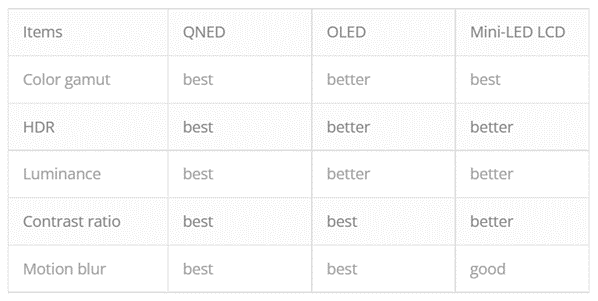
QNED is a self-luminous display and because it uses QD, it has the best color gamut, HDR, luminance, contrast ratio, and motion blur, etc., and is a product expected by Samsung Electronics.

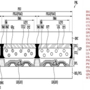
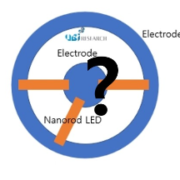
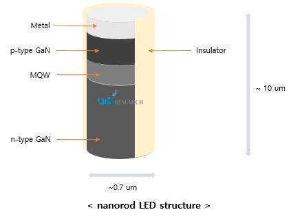
It can be confirmed by the structure that QNED is the display with the best characteristics. QNED consists of a pixel layer with a nano-rod LED on the TFT structure of 3T1C used in large OLEDs, and a color conversion layer consisting of QD and CF (color filter) on top.

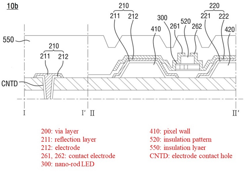
In OLED, electrodes (cathode and anode) and electrode line for transmitting a signal to a pixel are located above and below the light emitting material, whereas in QNED, both the signal transmitting electrode (pixel electrode) and electrode line are located on the same plane. In addition to the pixel electrode, the QNED additionally includes a reflective electrode to increase light output efficiency. The pixel electrode serves as an alignment electrode for aligning the nano-rod LED.

< QNED section structure >

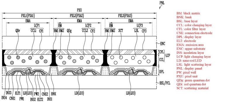
< QNED pixel structure >

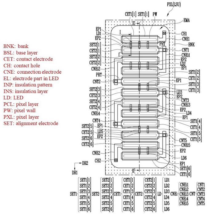
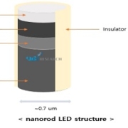
< QNED pixel planar structure >

Looking at the planar structure of a QNED pixel, a plurality of pixel electrodes are connected in series in one pixel, and a nano-rod LED is positioned between the pixel electrodes. The pixel electrode is on the pixel wall (PW) formed of an insulating material, and each pixel is surrounded by a bank (BNK) to separate regions.


The core technology of QNED is driving technology and sensing technology.

The driving technology includes a driving technique for aligning nano-rod LEDs and a driving technique for uniformly controlling pixels that may have a deviation in the number of nano-rod LEDs. The alignment circuit includes switching elements for each pixel, and the switching element applies an alignment signal to the pixel. The alignment state of the nano-rod LED is determined depending on which alignment signal is given to each pixel.

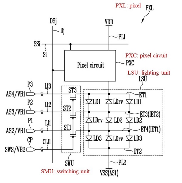
< Drive circuit for alignment >

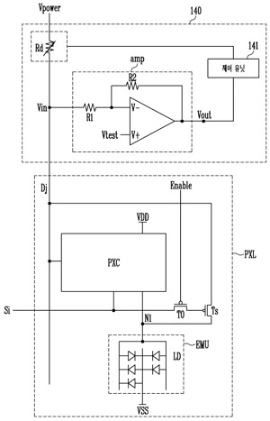
< Sensing transistor for checking alignment >

The most important driving technology is a technology that supplies current to each pixel so that the luminance can be uniform across the entire screen even if the number of nano-rod LEDs per pixel is different. It is a method of controlling each pixel based on the data read from the sensing transistor.

[QNED Technology Completion Analysis Report] details the sensing transistor, sensing wiring, and sensing signals that can check the nano-rod LED alignment status on the panel.


As sensing technology, there are sensing technology (sensing transistor) designed inside QNED and sensing technology used in QNED manufacturing. The sensing technology used to manufacture QNEDs is inherent in inkjet systems. There are three sensing technologies in the inkjet system: the number of nano-rod LEDs in the ink and the viscosity analysis of the solvent, the analysis of the number of nano-rod LEDs sprayed on the panel, and the analysis of the nano-rod LED alignment state.

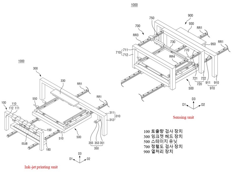
< Inkjet system configuration >

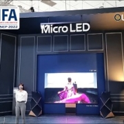
QNED has already proven that 4K 65 inches can be driven two years ago. Samsung Display is concentrating on finishing work to secure the screen uniformity of QNED.

How far has QNED completed?

The reality of QNED (quantum dot nano-rod LED), which Samsung Display is preparing as a next-generation display, has become clear.

As a result of analyzing 160 patents applied by Samsung Display, it was confirmed that the structure constituting the QNED has already been completed, and that the only remaining task is to keep the number of nano-rod LEDs arranged in the light-emitting pixel constant.

As a result of classifying the contents of each patent according to the purpose of the application, a total of 39 types were found, with 49 cases related to device arrangement being the most. The following is 20 cases to improve the light efficiency.

The number of aligned nano-rod LEDs per pixel, which determines the yield and image quality characteristics of QNED, is determined by the distribution of LEDs in the ink, the number of LEDs injected into the pixel, and the alignment ratio of the injected LEDs.

If the distribution of the number of nano-rod LEDs per pixel is different, there is a change in the voltage applied to each pixel, resulting in a defect.

It has been confirmed that Samsung Display has already developed a method for making the number of nano-rod LEDs per pixel constant and an algorithm that can make the luminance uniform even when the number of nano-rod LEDs is different.

In the “QNED Technology Completeness Analysis” published this time, it was written as the contents of the previous report published through analysis of 94 patents and 66 newly added patents. It was analyzed and recorded.

In this report, QNED patent numbers, classification tables, and quantitative analysis data that have not been disclosed before are provided in Excel.

Samsung’s QNED, will make a sensation in the TV and display markets?

QNED (Quantum dot nanorod LED), which is known to be under development by Samsung, is becoming a hot issue in the display industry in 2020.

With the emergence of micro LEDs, followed by CRTs, PDPs, LCDs, and OLEDs as TV displays, the industry is interested in whether QNED could be another new technology.

Samsung Display is known to stop the LCD business and invest 13.1 trillion won as an alternative to do the QD-OLED business. In this situation, attention is being focused because the development of QNED can act as another variable in the future of Samsung Display’s large display business.

QNED uses oxide TFT and QD (quantum dot) -CF (color filter) technologies used in QD-OLED manufacturing. On the other hand, the pixel material that emits light is characterized by being changed to a nano-sized bar-type LED (nanorod LED), unlike OLED emitting materials. The pixel manufacturing technology, which is the core technology of QNED manufacturing, is a method of spraying nanorod LEDs dispersed in a solution into a pixel area by an ink jet method and arranging them in a self-align method by an electric signal.

UBI Research published a report that analyzed the structure and manufacturing technology of QNED based on the patented technology filed by Samsung Display. This report is structured to quantitatively analyze QNED-related patents filed by Samsung Display, so that QNED’s technology completeness and mass productivity can be known.

QNED structure and manufacturing technology analysis report published

UBI Research (www.ubiresearch.com) published “QNED Structure and Manufacturing Technology Analysis Report”, which analyzed 41 cases of Samsung Display’s QNED (quantum dot nanorod LED) published patents.

The contents described in this report were selected from the 41 patents published, which are considered to be used for QNED manufacturing, and are constructed by qualitative analysis.

As a result of analyzing the published patent, the QNED structure was formed of TFT, pixel, and QD (quantum dot) -CF (color filter). In the published patent, all TFT structures are depicted as 2Tr (transistor), but it is estimated that a 3Tr1C structure will be used because at least three TFTs for current driving are required. The pixels consisted of nanorod LEDs, electrodes, and optical structures to increase light efficiency.

Until now, the electrode structure of the pixel was known to be rectangular, but as a result of analyzing published patents, the electrode structure is estimated to be circular. In a specific patent, when the asymmetric waveform was applied to the circular electrode, the alignment direction and alignment characteristics of the nanorod LED were improved. It is judged that the nanorod LED alignment electrode and the drive use the same electrode.

The nanorod LED used for QNED manufacturing is made of GaN and emits blue light, and the size is <1um x 10um. In order to increase the alignment effect of the nanorod LEDs and reduce process defects, the nanorod LED surface appears to be treated with an insulating film and an orientation radical.