OLED Market Enters Adjustment Period from Rapid Growth

As smartphone makers, including Samsung Electronics and Apple, increased the use of OLEDs in flagship models, the growth of the OLED market, which had been rapidly growing, has been braked.

The third quarter of each year is the season with the best OLED performance for smartphones due to the launch of a new iPhone. According to the display market track of UBI Research (www.ubiresearch.com), in the third quarter of this year, 113 million units were shipped, an increase of 26.3 million units compared to 86.7 million units in the last quarter, showing a growth of 30.4%. However, this figure is due to an optical illusion. The reason is that the results in the first and second quarters were very poor compared to before due to COVID-19. Compared to the third quarter of last year, shipments in the third quarter of this year decreased by 17.9%. Shipments are smaller than in the third quarter of 2018.

The decrease in OLED shipments for smartphones in the third quarter is due to the addition of Huawei sanctions to COVID-19. The sharp drop in shipments from Samsung Display and BOE to Huawei deteriorated the third quarter earnings.

There are also many analyzes that companies such as Samsung Electronics, Oppo, and Vivo will benefit from the reflection due to Huawei sanctions. However, since Samsung Electronics is currently struggling in the Chinese market, and the brand power of Oppo and Vivo is less than that of Huawei, it will be difficult to replace the expensive smartphone market in China occupied by Huawei. Therefore, Huawei’s smartphones, which mainly use OLEDs, disappear from the market, and shipments of Samsung Display and BOE are also forced to decrease more than expected.

The growth of the smartphone OLED market is expected to slow for the time being due to Huawei’s smartphone production disruption, which was expected to break through the 300 million units’ market and purchase OLED in large quantities. As a result, the OLED market in China will suffer a severe oversupply situation.

Samsung Electronics’ foldable smartphone to be released in 2021, with touch pen and UTG thickness different?

According to the ‘2020 OLED Components and Materials Report’ recently published by UBI Research, Samsung Electronics’ next-generation foldable smartphones to be released in 2021 are expected to be equipped with a pen function.

It is expected that the pen function will be added to Samsung Electronics’ Galaxy Z Fold2, which was released in September, but the flexibility issue of the digitizer, which is an essential material to support the pen function, and ultra thin glass (UTG), the cover window material. The pen function was not added in the end due to its thin thickness.

In order to add a pen function, Samsung Display seems to be considering applying an active electrostatic solution (AES) method that does not require a digitizer and changing the thickness of UTG.

First, the’Galaxy Note’ series uses an electro-magnetic resonance (EMR) method with a digitizer at the bottom of the OLED panel. The EMR method has good touch sensitivity and does not require a battery to be embedded in the pen, but it is not applicable to foldable devices due to the flexibility issue of the metal digitizer.

Unless the companies developing the EMR method provide a special solution, the AES method is highly likely to be applied to the pen for the next ball double device. In this case, the sensor pitch of Y-OCTA is formed more densely or the Touch IC is more complex. Can be designed.

The AES method is also being developed by LG Display and BOE to apply to foldable devices.

In addition, the thickness of UTG is also expected to change. The 30 um thick UTG, which is currently commercially available, has good flexibility, but due to its film-like characteristics, when pressure is applied with a touch pen, traces remain and may affect touch sensitivity. To solve this problem, Samsung Display is developing UTG with a thickness of more than 60 um in cooperation with glass processing companies.

As the thickness of the UTG decreases as the thickness increases, it is expected that the UTG currently under development will be applied with a concept in which the folded part is processed thin and filled with a material having the same refractive index as glass. In addition, in the future, there is a possibility that an additional coating process will be added after the reinforcement process without a protective film such as PET on UTG.

In UBI Research’s ‘2020 OLED Parts and Materials Report’, Samsung Display’s expected change in foldable OLED was written as a roadmap and the trends of related materials were analyzed. According to the report, Samsung Electronics’ application of pens for foldable devices is expected in 2021, and UTG materials are expected to lead the market at 78% by 2025 in the future cover window market for foldable devices.

LPKF’s laser glass processing technology, makes a cover glass thicker than UTG be folded.

It was expected that the S Pen would be applied to Samsung’s ‘Galaxy Z Fold2’, which will be released in the second half of this year, but it has passed the year.

UTG, the cover window material currently applied to Samsung Electronics’ ‘Galaxy Z Filp’, is 30 um thick and is 1/10 thinner than 300 um, the thickness of commercially available cover glass.

It was possible to have flexibility by using UTG into a foldable phone, but due to the film-like characteristics, there was an issue that durability was insufficient to apply the S Pen.

In order to handle this issue, a technology that increases the thickness of UTG and secures flexibility will be needed. A typical method is processing the folding part of the glass to get flexibility even at a thick thickness.

LIDE (Laser induced deep etching) technology, developed and patented by German high-tech company LPKF, is expected to be a good example. It is known that this technology is a two-step process called micro-region transformation and chemical treatment using a laser, and can process glass of various thicknesses from 30 um to 900 um without micro crack.

LPKF explains that the part where the cover glass is folded is finely processed with a laser to give flexibility to the glass, and it is possible to design the pattern to be invisible using a polymer having same reflectivity as a cover glass.

If you look at Vitrion’s YouTube video (https://youtu.be/Vh3rU4LRHaw), a separate brand related to LIDE, in LPKF, you can see that a cover glass with a thickness of 500 um was patterned to secure bending radius of 1 mm.

<LPKF foldable OLED cover glass, Source: LPKF>

With this glass processing technology, attention is paid to whether a S-pen can be supported as a thicker cover glass is applied to a foldable phone in the future.

Samsung Display A3 line replaced with Y-OCTA manufacturing line

The touch panel technology installed on a mobile phone is an important element technology that performs a user interface function. Touch technology is changed from an add-on type to an on-cell type in flexible OLED displays.

The built-in method in which a touch sensor is formed on a thin film encapsulation (TFE) is called by various names such as Y-OCTA(YOUM on-cell touch AMOLED), ToE(touch on encapsulation) or FMLOC(flexible multi-layer on cell touch) for each panel maker. Unlike the add-on type, the on-cell type touch sensor is formed directly on the top of the encapsulation layer without a separate base film. Due to this, the on-cell type has a higher process difficulty than the add-on type, but it is advantageous to manufacture a thin OLED panel thickness, and there is an effect of reducing the process cost.

Recently, in order to apply this on-cell type touch technology to mobile phones using OLEDs, each display manufacturer is undergoing a step-by-step line modification work. Four mask steps are added to apply the on-cell type touch technology. There are two ways to cope with this process step increase: to install and respond to new equipment as much as the process to increase, and to proceed with the process at existing facilities.

Samsung Display decided to use an existing exposure machine to use the on-cell type touch technology in the existing A3 line (Tangjeong), and is in the process of remodeling the 105K capacity TFT production line. In the existing process flow, a back plane process is performed with mother glass of 1500×1800 mm2 and 1500×900 mm2 glass with half-cutting of this mother glass is processed in the OLED process. Therefore, in order to process the half-cut glass again in the back plane equipment, the jig manufacturing method of connecting and processing two cut sheets is applied. After this modification, the production capacity of the A3 line will be reduced. The amount of 105K of the A3 line that is currently being renovated is changed from LTPS process to LTPO process, and it is combined with Y-OCTA process. In this case, 3 mask steps increase as LTPS is changed to LTPO, and 4 additional mask steps increase for Y-OCTA. As a result of the total increase of 7 mask steps, the A3 line is expected to reduce the existing 105K production capacity to approximately 75K level after remodeling.

China’s BOE is also constructing built-in touch processes in B7 and B11. BOE is in the process of adding and processing exposure equipment, etc. as a way to add a built-in touch process. In this case, there will be no significant change in production capa.

<Production capacity comparing with before/after modifying at SDC A3 line>

QNED structure and manufacturing technology analysis report published

UBI Research (www.ubiresearch.com) published “QNED Structure and Manufacturing Technology Analysis Report”, which analyzed 41 cases of Samsung Display’s QNED (quantum dot nanorod LED) published patents.

The contents described in this report were selected from the 41 patents published, which are considered to be used for QNED manufacturing, and are constructed by qualitative analysis.

As a result of analyzing the published patent, the QNED structure was formed of TFT, pixel, and QD (quantum dot) -CF (color filter). In the published patent, all TFT structures are depicted as 2Tr (transistor), but it is estimated that a 3Tr1C structure will be used because at least three TFTs for current driving are required. The pixels consisted of nanorod LEDs, electrodes, and optical structures to increase light efficiency.

Until now, the electrode structure of the pixel was known to be rectangular, but as a result of analyzing published patents, the electrode structure is estimated to be circular. In a specific patent, when the asymmetric waveform was applied to the circular electrode, the alignment direction and alignment characteristics of the nanorod LED were improved. It is judged that the nanorod LED alignment electrode and the drive use the same electrode.

The nanorod LED used for QNED manufacturing is made of GaN and emits blue light, and the size is <1um x 10um. In order to increase the alignment effect of the nanorod LEDs and reduce process defects, the nanorod LED surface appears to be treated with an insulating film and an orientation radical.

The next full-screen display trend is the under-display camera

Reporter : Daejeong Yoon

Since Samsung’s Galaxy S8 and Apple’s iPhone X launch, smartphones with the Home button removed have become a trend in the smartphone market.

Due to the nature of smartphones that cannot grow indefinitely, display sizes with a large proportion within limited smartphone sizes are directly related to the competitiveness of smartphone set makers.

Samsung’s Galaxy S10, which was recently released, attracted great attention with its flexible OLED with HIAA (hole in active area) technology. Notch or HIAA designs, however, can still interfere with video viewing and gaming because camera lenses occupy a small portion of the display.

That is why a number of panel makers are developing under display camera technology for a full-screen display.

Under display camera technology allows the front camera to be placed behind the display for a full-screen display. Oppo unveiled the first smartphone with the technology at MWC China 2019, and BOE and Visionox also anticipated that under-display cameras will become the next trend in smartphones at CIOC 2019.

It is expected that screen, camera module, and algorithmic technologies will all be specially designed to implement under display camera technology. Specifically, the technology to make the pixel near the camera at low resolution to secure transmittance, to mount a CMOS image sensor of a larger pixel size than the existing, and to apply algorithm technology to improve the picture quality.

The trend of full-screen smartphones, which began in 2017, is paying attention to whether full-screen smartphones will bloom with the technology of under-display cameras since 2020.

[28TH FINETECH JAPAN] Sharp, announced Future Strategy Combining IGZO and OLED

Mr. Atsushi Ban, Vice President of Sharp presented a future strategy that combines IGZO and OLED through a keynote session at the 28th FINETECH JAPAN, held in Makuhari Messe, Japan from December 5, 2018.

Ban emphasized “The proportion of OLED in the entire display market is expected to grow even higher, and the new value of OLED is no different than flexibility.”

He said, “Sharp is also planning a variety of applications using the thin, light-weight and flexible characteristics of OLED. From the third quarter of 2018, its Taki plant has produced 4.5G backplanes and the Sakai plant is under injecting glass for OLED and module processing for 4.5G 15K quantity.”

Ban also pointed out the possibility of expanding the OLED industry through flexible OLED, commenting that Sharp’s next goal is to develop foldable OLED that combines IGZO. Sharp has pioneered a new display technology, called IGZO, which has been known for its semiconductor properties for years, but Sharp has developed a crystalline form that maximizes its benefits for greater display performance, and IGZO improves the performance of display panels in three significant ways: lower power consumption, higher resolution and special benefits for touch-sensitive displays. Ban expected that it could create new value if IGZO is combined with medium to large sized foldable OLED or rollable OLED.

Finally, Ban introduced Sharp’s IGZO development roadmap and announced that it will develop much improved IGZO.

Apple adopts LTPO TFT to extend battery life time to Apple Watch Series 4

Reporter & Analyst : Daejeong Yoon

Apple released its Apple Watch Series 4 with enhanced healthcare features on a larger screen than before, in the Steve Jobs Theater at Apple Park in California, USA on September 12.

<Apple Watch Series 4, Source: Apple.com>

In this announcement, Apple brought Apple watch series 4 with a new technology called LTPO to improve power efficiency.

LTPO stands for low temperature polycrystalline oxide. It is a kind of TFT using only the advantages of poly-Si with good charge mobility and IGZO with low power driving. LTPO TFTs have low leakage current and good on / off characteristics, which lowers power consumption and increases battery life.

<Apple’s LTPO TFT patent>

In addition, Apple increased the size of its Apple Watch 4 to 40mm and 44mm. The edge-to-edge screen is 35% and 32% larger than previous models by narrowing the bezel compared to previous models. The screen resolution was 368×448 pixels for the 44mm model and 324×394 pixels for the 40mm model. The display of Apple Watch4 is a plastic OLED made by LG Display with a maximum brightness of 1,000 nit. The Apple Watch Series 4 starts at US$399 for GPS model, while the cellular model starts at US$499. The Apple Watch Series 4 is available for pre-order from Septmber14 in the U.S. with the availability beginning September 21.

OLEDON, is to announce belt-plane source deposition technology for manufacturing ultra-high resolution and ultra-area OLED

Plane source technology, which was first developed by OLEDON in the world, has the principle of depositing the first organic material on the metal surface and evaporating it upwards to produce fine pattern of 2250 ppi, which is ultrahigh resolution. In this plane source process, three processes such as the first deposition, the plane source inversion, and the second evaporation are necessary, and the number of the high vacuum chambers is increased when the mass production is applied. The belt plane source FMM deposition technology introduced by OLEDON has a concept of carrying out the above processes at a time in one evaporation equipment. This is a continuous plane source supplying deposition technology in which the metal surface is formed in a belt shape.

Hwang added, “Using vertical plane source enables smooth deposition process for the 12th generation class area substrate for QD-OLED TV without sagging problem. Vertical belt-plane source evaporation equipment adopts the concept of depositing the substrate in a standing-up position so that the load on the framed glass chuck and the open mask is very low. Thus, easy transportation of the substrate, and uniform deposition process of thin film over a very large area in the static state are possible.” This technology is expected to be applicable not only to the 8th generation but also to the cluster type mass-production evaporator with substrate sizes more than 10 generations in the future.

<Vertical belt plane source evaporator for QD-OLED, Source: OLEDON>

Commenting finally that the company has successfully completed the material denaturation test for blue materials and the blue dopant deposition test, Hwang expected the plane source deposition technology to be applied to both small & medium sized OLED and large area OLED manufacturing in future.

On the other hand, OLEDON holds more than 30 related patents including original patents of plane source and belt plane source evaporator. Also, the company recently filed a patent related to a vertical belt plane source evaporator for mass production.


OLEDON unveils plane source deposition technology for ‘super-gap’ OLED manufacturing.

Attention is growing since OLEDON, a venture company developing OLED deposition equipment, unveiled plane source deposition technology for OLED manufacturing to maintain ‘a superb gap with the competing countries’, at IMID2018, held in COEX, Seoul, Oct. 24, 2018.

Hwang Chang-Hoon, CEO of OLEDON, said, “Korea should actively invest in the development of creative deposition technology to maintain the first place in the current OLED producing countries.” He expects that plane source deposition technology is to be used both for small and medium size OLED and large area OLED manufacturing in future.
OLEDON is developing the world’s first curved plane source FMM deposition technology, which is an ultra-high-resolution OLED deposition technology capable of manufacturing 2250ppi AMOLED. The shadow distance of fine pattern can be up to 0.18um, enabling 11K high-resolution AMOLED pattern process.

<Existing FMM deposition pattern (left) and plane source FMM deposition pattern (right), Source: OLEDON>

According to Hwang, this process was confirmed with 800 ppi shadow mask, and the emission area of the pattern deposited with plane source was 1.7 times higher than the conventional deposition method.
On the other hand, OLEDON holds the original patent for the FMM deposition technology of plane source, and has recently applied for a patent for vertical plane source deposition for large area OLED TV manufacturing.

<Vertical plane source deposition for OLED TV manufacturing, Source: OLEDON>

OLEDON develops vertical plane source deposition technology for large OLED TV manufacturing

Hwang Chang-Hoon, CEO of OLEDON, which has developed plane-source deposition technology for small & medium-sized OLED and large area OLED, said that it is under development of vertical plane source deposition technology capable of manufacturing ultra-large OLED TVs of 77 inches or larger. Hwang introduced the related technology that it is possible to mass produce OLED TVs of 77 inches or more without the sagging problem of large substrate such as 12th generation (3300 x 4000 mm) substrate when using vertical plane source deposition technology.

According to Hwang, the production yield for 75 inch TVs or larger with the conventional inline type evaporator might be very low due to severe sagging of the substrate and difficult control of many linear sources. To solve this problem, Hwang said that a new 12-generation large-area cluster-type deposition technology is needed, and that vertical plane source deposition technology will be an appropriate alternative.

On the other hand, OLEDON holds the original patents for plane source deposition technology. It also filed a patent related to the curved plane source FMM deposition for high-resolution AMOLED manufacturing, and a patent related to the vertical plane source deposition technology for manufacturing large-area OLED TV.


LG Display “Strategic direction is OLED. Uncompetitive LCD lines are planned to be switched.”

In the 2Q earnings release conference call hosted on the 25th July, Kim Sang-don, LG Display CFO, said, “Looking back at the first half of 2018, the market was in a difficult situation due to the slump in prices, the traditional off-peak season and increased display supply from China. We expected the market conditions to be stabilized in the first half of this year from the bad market condition of the second half of last year, but it has continued to decline more rapidly and steeply. However, with starting the second half of 2018, it has been observing that the price is rising since July owing to upcoming favorable seasonality and customer restocking.”

“Although the market situation has changed favorably in the second half of the year, it is different from the past supply and demand cycle because of the uncertainty of forecasts. Moreover, the oversupply and asymmetric competition in the display market are unavoidable.” LG Display announced that it will maintain its conservative strategy in the second half of the year as the unpredictability is still high.

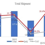
LG Display’s sales revenue in the second quarter of 2018 was KRW 5,611 billion, decreased by 15% compared to the second quarter of 2017. Operating loss in the second quarter of 2018 recorded KRW 228 billion. This compares with the operating loss of KRW 98 billion in the first quarter of 2018 and the operating profit of KRW 804 billion in the second quarter of 2017. The company suffered a large deficit due to a continued and steep decline in panel prices and lower demand in panels following the previous quarter. Although the shipment was increased by 2% QoQ, the selling price per area (m2) was decreased by 4%.

As a positive indicator, the TV panel price fell sharply, but the overall panel price decline was only 1% due to the competitive position of OLED panels. The market is anticipated to turn into positive situation in the third quarter, compared to the first half of the year, since panel shipments are expected to increase with the orders to restock the inventory.

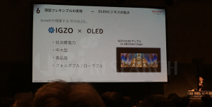
LG Display, which is currently conducting both LCD and OLED business with small and medium sized panels and large area panels, mentioned clearly about its future strategic direction including the direction for the second half of the year as “concentrating on OLED business and focusing on high value of LCD business” in this conference call.

LG Display announced that it will focus more on differentiated LCD features and technologies in the IT sector such as narrow bezel, IPS borderless, and oxide technology, as well as high-value-added products such as larger-size TV panels and commercial displays, considering that a structural oversupply in panels and fierce competition among display makers are expected to continue down the road.

In addition, LG Display will achieve a turnaround to profit in the OLED TV sector in the third quarter of 2018. By making its final decision to invest in its Gen 10.5 OLED panel production line in Paju, Korea, and by starting mass production in the latter half of 2019 at its Gen 8.5 OLED production line now under construction in Guangzhou, China, LG Display will accelerate the expansion of the global large-size OLED market. Furthermore, additional production facilities for OLED 8.5 generation are known to be considered with the plan that the rationalization of LCDs during the year is also to be implemented although there was no direct mention of the timing and specific lines. For the plastic small and medium-sized OLED panel business, which is experiencing difficult times, compared to large area OLED, for which LG is expanding the production capacity in response to increasing demand, it said that they are preparing for future markets with the necessary strategic technologies with the emphasis of mobile and automotive markets. The E6-1 line, which has been mentioned as a production plant for Apple, is expected to begin mass production in the fourth quarter of this year, revealing the possibility of a possible supply of display to the iPhone OLED model in 2018. In addition, demand for OLED panels is increasing in the automobile market, and it is expected that full-scale business will start in the second half of next year. At the current order backlog, it is confirmed that OLED panels are in the late stage of about 10%. This means that much of the work has already been done. Finally, LG Display is well aware of the lack of funding and funding shortfalls over its competitors in relation to its future preparations. The company plans to reduce its capex by about 3trillion won by 2020, with a substantial portion of depreciation and amortization It is possible through internal working capital management and it plans to borrow the rest. LG Display confirmed that it has not reviewed the rights issue several times in the market, and LG Display has thoroughly prepared a variety of OLED portfolios, revealing its commitment to success by differentiating it from its competitors in the area of latecomers.

Sony, announced the commercialization of 0.5-inch micro OLED with UXGA resolution

Sony announced the upcoming release of the ‘ECX339A’, a 0.5-inch OLED micro-display with UXGA resolution. According to Sony, it has achieved the world’s smallest pixel pitch of 6.3 μm, enabling a resolution 1.6 times higher than its predecessor, “ECX337A “(0.5-inch QVGA (1280 × 960)).

<Sony’s 0.5 inch micro OLED ‘ECX339A’, Source: sony.co.jp>

By employing newly-designed peripheral circuits that operate on half the voltage of previous model, it supports a high frame rate of up to 240 fps, with dual line progressive driving technique and low power operation.

<Comparison of OLED resolution between new product(left) and previous product(right), Source: sony.co.jp>

According to Sony, the high resolution of the existing micro display had problems such as deterioration in picture quality and deterioration in viewing angle due to pixel pitch reduction; however, they have been improved by Sony’s transistor layout, process optimization, and compensation circuit. In addition, the color filter is deposited directly on the silicon substrate, reducing its distance from the light emitting layer, and the filter’s color array has been modified to secure the viewing angle properties while achieving high resolution.

<Structure and viewing angle image, new product (left) and previous product (right), Source: sony.co.jp>

The mass production schedule for the ECX339A is November 2018, and the sample price is set at JPY 50,000 (Tax not included). Sony expects this product to be applied to high-end cameras and head-mounted displays for virtual reality, which require the highest picture quality.

<ECX339A, key specifications, Source: sony.co.jp>

QD-OLED TV, is it to be the next generation premium TV?

Samsung Electronics is currently occupying the premium TV market with QD-LCD TVs, which use ‘PL-QD (photoluminescence quantum dot) technology’. This technology has a mechanism in which the material stimulated by external light re-emits light.

The operating profit of the consumer electronics division (CE), which controls QD-LCD TVs, fell more than Korean won 1 trillion in last year and the operating profit ratio was only 3.6%.

On the other hand, LG Electronics’ HE business division achieved a record operating profit of Korean won 1,566.7 billion and an operating margin of 8.1% through OLED TV. Sony also turned its operating profit into a surplus by quickly taking over the premium TV market with OLED TV.

OLED TV has had a positive effect in driving corporate sales growth.

Samsung Electronics has been developing EL-QLED, with EL-QD (electroluminescence quantum dot) technology, to increase its market share in the premium TV market. However, efficacy, lifetime and mass production technology of quantum dot, which is the material of QLED, is not yet secured.

Recently, QD-OLED TV technology, which uses blue OLED as a light source and that implements red and green colors through a quantum dot color filter (QDCF), is attracting attention.

<Expected structure for QD-OLED, Source: Samsung Display Blog>

By using QDCF, it is possible to easily make desired colors by adjusting the size of the QD material and improve the color reproduction rate. This is because the color gamut is enlarged to BT2020, so it is close to natural color and it is possible to deliver vivid picture quality more clearly. In addition, QD-OLED TV has a top emission structure, which makes it easy to secure the aperture ratio, thereby improving resolution and screen uniformity.

However, in QD-OLED TV, there are various problems to be solved such as lifetime and efficiency of blue OLED, and technology of ink-jet printing process. Given that the industry is still in the early stages of reviewing the business possibility, QD-OLED TVs are expected to go into mass production after 2020.

Attention is focused on the QD-OLED TV’s entry into the premium TV market and its impact.

V-technology, announces acquisition of Lumiotec, OLED lighting company, and establishment of new subsidiary to develop next-generation OLED mask and deposition technology

V-technology said on February 7 that it would establish an ‘organic electronics business demonstration facility’ in Yonezawa, Yamagata Prefecture to develop a fine hybrid mask (FHM), which is next-generation deposition mask for OLEDs, and next-generation deposition technology.  The total investment is planned to be about 5 billion Japanese yen for two to three years. The facility is scheduled to be completed in August, 2018 and the mask samples are to be shipped from October, 2018.


V-technology’s FHM adopts electroforming method and non-tension structure which is different from conventional FMM manufacturing method. The weight of the mask produced by this FHM method can be reduced to one tenth (1/10) level compared to the existing conventional mask. As the weight decreases, the problem of mask bending due to its own weight and shadow interference problem caused thereby can be solved. V technology already unveiled a Fine Hybrid Mask (FHM) that can implement 738ppi UHD at Finetech Japan 2017 in April 2017.

<V technology, Fine hybrid mask with non-tension structure>

V-technology also announced that it has reached a basic agreement to transfer the entire stock of Lumiotec, a lighting OLED panel company. Lumiotec is specialized in lighting OLED panels in Japan, and has supplied a large number of OLED lighting panels for indoor use and exhibition use in addition to indoor lighting.

<Lumiotec lounge lighting, Source: Lumiotec>

V technology expects Lumiotec’s technology and business know-how to contribute to the group’s development. The stock transfer is scheduled for April, and information such as the transfer price is not disclosed.


[iMiD 2017] JOLED announces printing-type OLED development trend and future road map

At the ‘IMID 2017 Business Forum’ held in COEX, Seoul from 18th to 19th, Toshiaki Arai, chief technologist of JOLED announced JOLED’s printing technology and future road map.

<JOLED’s Toshiaki Arai chief technologist>

Toshiaki Arai, chief technologist stated that a stable jetting technology at 220 ppi level has been currently secured; high resolution OLED with more than 300 ppi has been developed at Gen 8.5 but there are some issues such as jetting accuracy and stability.

Toshiaki Arai introduced TG-TAOS (top gate-transparent amorphous oxide semiconductors) TFT, which will contribute to saving the unit cost of OLED with excellent performance at low price.

He also announced the future strategy of JOLED, stressing that, instead of small and large OLED dominated by South Korean companies, the middle-sized OLED for tablet and monitor with more than 200 ppi. Joled is the only OLED panel maker that unveiled its 21.6 inch 4K RGB OLED in 2017, using printing process, and has pilot launched.

<JOLED’s 21.6 inch 4K OLED in application of printing method>

On the other hand, according to the Nihon Keizai newspaper in Japan, JOLED is reported to have invested 100 billion yen in mass production of printing-type OLED. In addition, Toshiaki Arai stated that the OLED test samples manufactured by printing process have been provided since this April and the mass production will realize in the second half of 2018.


Is there possibility of High resolution(UHD) OLED Smart-phone generation?

Recently VR contents experience through smart-phone device has been increased, therefore high resolution of smart phone is becoming necessary. However, OLED smart-phone resolution still remains at QHD level for 3 years since QHD OLED is applied to Galaxy Note 4 for the first time in 2014.

The core point that decides resolution of OLED smart-phone is evaporation process for emission layer. Bottom-up type evaporation method, which is applied to the recent devices is that substrate and FMM (fine metal mask) are horizontally arranged on the upper side of evaporator and vaporize the organic material from the lower linear source in order to form RGB layer.

Thin FMM measures less than 15um thick is necessary for making high resolution OLED like UHD level, however, as FMM gets thinner, it would be difficult to make mass production because technical problems will be occurred such as patterning, sealing and welding.

In order to solve these problems, various metal mask patterning technologies are being developed such as vertical type evaporation and plane source evaporation.

Vertical type evaporator that arranges board and FMM vertical is developed by Hitachi of Japan for the first time. And Canon Tokki exhibited Gen6 vertical type evaporator at Finetech Japan 2013, however it is not being used for mass production at the moment.

<Canon Tokki’s Gen6 vertical type evaporator which is exhibited at Finetech Japan 2013>

According to the recent ETNEWS, Applied Materials developed Gen6 flexible OLED vertical type evaporator and it is being tested in Japan Display.

Plane source evaporator is being tested but also the linear source type. Plane source evaporator method is that an organic material is first evaporated on the metal surface to produce plane source, then re-evaporated in order to form an organic thin film on the substrate.

In the past iMiD 2017, representative of OLEDON, Chang Hoon Hwang mentioned that 2250 ppi resolution OLED can be implemented through plane source evaporator.

For metal mask patterning technology, electro forming and laser patterning technology is highlighted. Electro forming method is developed by Wave Electronics, TGO Technology, Athene and so on. Laser patterning technology is being developed by AP Systems.

As such, development for high resolution OLED is receiving great attention whether it can solve the current problems and contribute to UHD resolution implementation for OLED smart-phone.

<Principle of plane source evaporation developed by OLEDON>

AUO unveils round OLED and foldable OLED for the smart watch in Touch Taiwan 2017

AUO showed the OLED that can be collapsible and three kinds of round OLEDs (1.2-inch, 1.3-inch, 1.4-inch) for the smart watch in Touch Taiwan 2017 held on 20th.

The round OLEDs in 1.2-inch and 1.4-inch of AUO are 326ppi, and it lowers an electric consumption at 30% versus former production goods. AUO also improves the visibility capacity in outdoor by embedding the brightness increase mode to make a display screen of two kinds of round OLEDs be clear even under bright sunlight.

The 1.3-inch OLED aimed at the smart watch for kids is light in weight, and strengthens the usability with a power saving mode and an intuitive touch interface function.

AUO displays two types of 5-inch flexible OLEDs that can be rolled or folded. Such two types of 5-inch flexible OLEDs apply the plastic board and AUO self-developed structure (special structural layer).

<AUO, 5 inch foldable OLED touch panel>

The 5-inch foldable OLED combines a flexible touch screen sensor that is developed by AUO itself.  The company said “it would provide excellent image quality, even if the curvature radius of the folded part is 4mm and less”.

For 5-inch rollable OLED, they explained “The thickness of the panel is just 0.1mm and only 5g. This model with the rolling radius of 4mm will provide wide color gamut”.

In last SID 2017, AUO has announced about that they applied the structure locating the TFT (Thin Film Transistor) and TFE (Thin Film Encapsulation) at the neutral axis to stand the compression stress or tensions during being folded.

Material Science to develop blue dopant for OLED … OLED Efficiency ⋅ Lifetime Up↑

A Korean venture company has succeeded in developing blue dopant for Organic Light Emitting Diodes (OLED) that a Japanese company has had its exclusive patent for. The dopant is an element that improves efficiency and life time by mixing with host that actually colors within the OLED.

In the meantime, many domestic material companies have developed OLED host, but it is the first case that a venture company has independently developed dopant on a commercial scale without receiving any support of large corporations.


Material Science (CEO Lee Soon-chang), an organic material developer for OLED has developed a technology that can replace Japanese I Company’s patent for blue dopant. Established in 2014, Material Science is supplying HTL( Hole Transporting Layer) and ETL (Electron Transfer Layer) to OLED panel makers.
Half of the 50 employees are R&D personnel. Last year, its sales were 6.6 billion won, and it is expected to exceed 10 billion won this year.

This time, due to the development of blue dopant by Material Science, OLED panel companies have an alternative to supply blue host and dopant besides I Company.

Japanese I Company has been developing blue dopant since 1995. At present, the company has more than 30 patents related to blue dopant (based on Japanese application for a patent), and its major 8 patents are valid until 2034. In particular, it has an exclusive patent for the combination method of blue dopant that includes blue host and pyrene with an anthracene structure (a compound in which three benzene rings are sequentially bonded). For this reason, the panel makers which purchase dopant from I Company must buy its host. If they mix I Company’s blue dopant with another company’s host, it is inevitable to infringe the patent in the case a host material has an anthracene skeleton.

Both Samsung Display and LG Display have been using I Company’s blue dopant and host.

The blue dopant developed by Material Science is designed to make molecules that are completely out of I Company’s compound patent. Conventionally, the method of applying an electron acceptor to a molecule has been used to improve the efficiency and lifetime of OLED and have a blue color.
On the other hand, Material Science introduces electron donor into molecules to improve the efficiency and lifetime while generating dark blue color. This dopant greatly reduces the solvent-dependent color development (solvatochromism) where emission wavelength changes due to the polarity of the surroundings. Therefore, the change of emission wavelength is also greatly reduced.

Jung Jae-ho, a researcher at Material Science said, “We have developed a new structure and a synthesis method, which makes it possible to produce its differentiated dopant.” “Panel companies are now able to utilize various types of blue hosts”. In addition, Material Sciences has been recently developing TADF(Thermally Activated Delayed Fluorescence) that OLED panel makers are struggling to introduce for the longer life of blue-emitting phosphors.

<OLED emitting material market forecast, UBi Research>

According to UBi Research, the OLED organic market is expected to reach $ 3.36 billion by 2021 (about 3.8 trillion won). And blue materials account for 11.5% of total sales.

[iMiD 2017] Samsung Display, Huge release of application using OLED

Samsung Display has received great attention by releasing a large number of applications using OLED such as VR and light field display in iMiD 2017 held in BEXCO, Busan from 28th to 31st August.

<Samsung Display booth>

First, Samsung Display comparatively exhibited a 3.5-inch OLED with 460ppi resolution for virtual reality and an 806ppi 3.2-inch OLED. A company official said “The higher the ppi, the better the experience of realism and immersion,” and mentioned “We are currently developing higher resolution OLEDs.”

<Comparison of 3.5 inch 460 ppi OLED and 3.2 inch 806 ppi>

In addition, Samsung Display exhibited OLED light field displays in the future display zone, and in the AMOLED zone, visitors can directly compare LCD and OLED.

A company official explained that “light field display is a technology that implements 3D by applying an optical lens on a panel, which is a little different from hologram using light interference effect.” And he said “We are developing a viewing angle that is wider than 30 °,” revealed “We now have pixel and lens alignment issues and optical design issues.”

<OLED light field display description and specification>

In the AMOLED zone, panels were displayed to directly compare the contrast ratio of LCD and OLED. The contrast ratio and color expressiveness of the OLEDs were clearly different from those of the LCDs, and a company official said, “These differences are the reasons why OLEDs are used in the Galaxy series.”

<Comparison of OLED (Left) and LCD (right) image quality>

Samsung Display has also introduced 1.3 inch circle OLED and 12 inch FHD OLED, which led to the great interest of the visitors during the exhibition.

[iMiD 2017] LG Display, Spur Development of 77 inch transparent flexible OLED

LG Display’s Kwon Se-Yeol senior researcher introduced the 77-inch transparent flexible OLED which had been introduced in June at IMID 2017 held in BEXCO, Busan on Aug. 30, and announced the applied technologies to realize this.

Kwon Se-Yeol senior researcher mentioned, “OLED is self-luminous, so it can be manufactured with a thin thickness because it does not need a back light unit. The thinner the thickness, the more flexible the OLED can be so that it is easy to implement flexible displays with OLEDs.” and forecasted. “It can be used in various fields such as signage and smart desk.”

The 77-inch transparent flexible OLED which is released this time is a top emission type for improved luminance. The transparent thin film encapsulation layer is applied, different from the conventional OLED TV or large flexible OLED, and two polyimide substrates are used.

Kwon Se-Yeol senior researcher said “We applied a transparent thin-film encapsulation layer instead of the existing metal encapsulation layer for the top emission method ” and explained “A white OLED light emitting layer and a color filter layer were formed on two polyimide substrates and cemented together. A barrier film and a multi-barrier were applied to the top and bottom of the polyimide substrates to prevent moisture and oxygen penetration.”

The Kwon Se-Yeol senior researcher then states that “flexural rigidity of the panel is mainly affected by the thickness of the polarizer and the encapsulant layer, so it is necessary to reduce the thickness in order to improve the flexibility”, and emphasized “By reducing the thickness of the encapsulant layer from 100 μm to 20 μm, we can reduce the strain on the OLED module from 0.36% to 0.21%, along with improved flexibility”.

In addition, he mentioned that surface reflection due to polyimide birefringence phenomenon, laser wavelength selection according to polyimide properties in LLO (laser lift off) process, and use of flexible OLED module are all covered, and technical development is continuing.

Meanwhile, LG Display has developed the world’s first 77-inch transparent flexible OLED with UHD (3840 × 2160) resolution, transmittance of 40%, and radius of curvature of 80R as part of the national project.

[iMiD 2017] OLEDON, Disclose plane source FMM deposition principle for 2250ppi OLED manufacturing

Prof. Hwang Chang-Hoon, CEO of OLEDON, a venture laboratory of Dankook University, presented a plane source FMM deposition technology capable of implementing 2250 ppi at iMiD 2017 held on the 28th.

According to Prof. Hwang Chang-Hoon’s presentation, the plane source deposition technology developed by OLEDON differs from the existing organic material deposition method. The plane source FMM deposition technique is that the organic material is first deposited on the metal surface to form a donor film and then re-evaporate it to form an organic thin film on the substrate. Applying this technique, organic matter forms a vertical gas beam due to plane evaporation. (Source patent: 1012061620000 Republic of Korea)

The shadow distance when organics are deposited with a plane source developed by OLEDON is 0.38 μm – 0.59 μm. This is a level at which a 2250ppi device having a pattern size of 4 um can be manufactured.

Prof. Hwang Chang-Hoon explained ‘applying the plane source deposition technique reduces the incidence angle of the organic material and dramatically reduces the shadow caused by the mask’. In addition, ‘using a plane source, the perpendicular organic gas beam can form a completely zero incident angle, so theoretically, the shadow distance can be zero um’.

<Principle of plane source deposition technology developed by OLEDON>

In addition, Prof. Hwang Chang-Hoon emphasized that ‘plane source deposition technology is essential for high-resolution shadow masks’.

For linear source FMMs currently in production, the shadow mask opening distance is 80 μm. As a result, the incidence angle of the organic material gas is inevitably large, making it difficult to produce a shadow mask having a high density pattern.

Prof. Hwang Chang-Hoon explained, ‘Using plane source deposition technology, shadow mask taping angle is 80 ° level’, and the distance between openings can be reduced to less than 20 μm so that plane source deposition techniques can solve the mask pattern density problems of linear sources’.

OLEDON is challenging fully shadow-free patterning conditions with plane source deposition technology, and plan to develop and install a plane source FMM evaporator capable of manufacturing 11K class micro OLED devices in cooperation with Prof. Jin Byung-Doo in Dankook University. (Reference: Homepage of OLEDON www.oledon.co.kr)

<The opening density change of the shadow mask when the plane source FMM deposition technique is used>

Meanwhile, OLEDON has 13 registered patents for plane source FMM deposition for mass production. Based on recent research results, they filed 7 new patents for mass production equipment in Korea and 3 applications are filed for PCT international application.

[iMiD 2017] AP Systems, Find FMM answers through USPL

At iMiD 2017 in BEXCO, Busan on 28th, AP Systems announced that it succeeded in developing 1000ppi FMM with USPL (ultra-short pulse laser).

Since FMM plays a role of depositing pixels and RGB organic materials, FMM serves as a factor that determines resolution and yield of OLED. At present, FMM is mainly manufactured by etching method. This method has a problem that a shadow phenomenon due to the precision, thickness, and weight of the fine pattern occurs, in order to solve this problem, various FMM manufacturing processes such as laser processing and electro-forming have been developed.

Among these, laser processing method has an issue of forming burrs around pin-holes due to the thermal effect caused by laser irradiation. These burrs increase the shadow interval of the FMM, which causes overlapping of patterns during RGB organic deposition, thereby degrading the resolution of the OLED.

AP Systems has developed a burr-free laser process that does not have burr phenomenon and further controls the taper angle.

The Burr-free laser process is a short-time irradiation of unidirectional pulses at a constant number of times, since the laser is not continuously irradiated, it minimizes accumulated heat energy and prevents burr formation. In addition, by controlling energy of the laser, it accumulates energy and forms taper.

In this way, AP Systems explained ‘they produced FMM with various shapes of fine pin-holes such as square, diamond, and polygonal shapes, as well as 1170ppi FMM’, and ‘’We also developed large-area FMM manufacturing equipment with USPL method’.

AP Systems also added ‘multi-beam and USPL is equipped for FMM manufacturing equipment so that it can improve productivity and realize UHD’.

Since the launch of the Galaxy Note4 in 2014, the OLED resolution has remained at the QHD level yet. In order to manufacture an OLED having a high resolution (UHD level or higher), it is necessary to solve various technical problems faced by FMM. Accordingly, it is noteworthy how USPL technology of AP Systems will affect the future OLED market.

<1000ppi FMM produced by AP Systems>

<various type of FMM produced by AP Systems>

[iMiD 2017] TCL, Development focusing on Solution process OLED and QLED

TCL’s Xiaolin Yan CTO addressed solution process OLED TV and self-emitting QLED TV as premium TV after white OLED TV at iMiD 2017 keynote address in BEXCO, Busan on 29th.

Yan CTO noted that white OLED TV, which is currently leading the premium TV market, meets all the requirements of premium TV due to its superior image quality, design differentiation, high resolution realization and nature-friendly characteristics compared to QD LCD TV.

In addition, the price that is higher than the current QD LCD TV is expected to be overcome by applying the solution process, and mass production is also expected in 2019.

Yan CTO predicted that the “solution process would be easy to produce 75-inch panels at Gen 10.5 because the process can be performed without splitting the ledger,” and “it is also possible to produce full-emission RGB OLED TVs.” However, he emphasized that the compatibility of materials and equipment and the development of ink forming process technology should be done.

Following to that, “QLED structure is very similar to OLED structure, so it is easy to apply the technology because of the low entry barriers,” he said. “The lifetime and efficiency of the blue light emitting layer compared to the current OLED is very low, and performance must be ensured without the use of cadmium.”

Lastly, He mentioned the establishment of printing technology in Guangdong JUHUA to promote the commercialization of solution process OLED TV and self-luminous QLED TV, and emphasized the cooperation of material, equipment and panel makers to develop next-generation premium TV.