Posts

[K-Display 2022] FMM Exhibition of Core Materials for OLED Deposition That are Leading in Localization

The K-Display 2022 exhibition, a Korean display industry exhibition was held at COEX in Samseong-dong from August 10 to 12.

Display-related materials, equipment, and parts companies such as Samsung Display and LG Display participated.

As OLED business is expanding from Smartphones and TVs to IT such as Notebooks, Tablet PCs and Micro OLED, related parts makers drew attention in exhibitions.

FMM for OLED Mobile(6GH)/ Philmaterials

FMM for OLED Mobile(6GH)/ Philmaterials

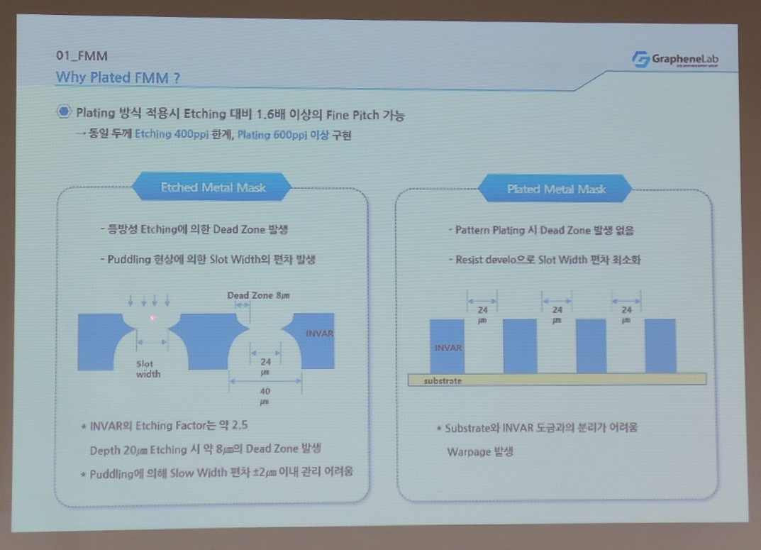
Invar, which is used for metal masks, is an iron-nickel alloy material necessary for manufacturing FMM for depositing RGB in OLED manufacturing.

Phillmaterials is using Invar as an ultra-high resolution display material because it has a low thermal expansion rate and thin thickness using the electroplating method.

Pixel Shadow can be improved compared to the compressed FMM. 6G half-sized OLED mobile masks and IT masks were also displayed.

Unlike the existing FMM method, Olum Materials used a method of attaching individual cells to a frame.

It is effective in preventing sagging in a large area, and if a mask is defective, it has the advantage of not replacing the entire mask.

Olum Materials exhibited a mask of 6G half size, they are developing it in the lead of localization.

FMM/ Olum Material

FMM/ Olum Material

FMM for micro OLED/ APS Materials

FMM for micro OLED/ APS Materials

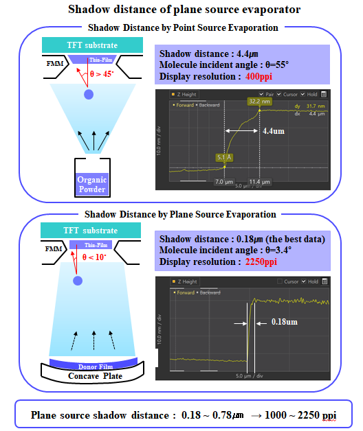
Because FMM for micro OLEDs requires finer holes, APS Materials introduced patterning laser technology using high-power lasers, the 2,050 ppi FMM, which can pattern on 8-inch wafer substrates used in display fields for AR and VR.

▶ 2022 OLED Component and Material Report Sample Download

GrapheneLab surpasses the ppi limit with a plated metal mask

GrapheneLab, a graphene commercialization technology company, announced that it is possible to manufacture FMMs over 800ppi using graphene.

At the ‘UBI Research First Half 2022 OLED Settlement Seminar’ held at COEX in Samseong-dong, Seoul on the 23rd, GrapheneLab CEO Yong-duk Kwon said, “In the early 2000s, FMM technology, which started in the early 2000s, was not interested in the plating method. It is changing,”, and “After 2013, many patents related to the plating method FMM manufacturing technology have been applied, and it is easier to apply the plating method than the currently used etching method in order to go to high resolution.”

Next, CEO Kwon said, “We moved away from the existing limiting etching method FMM and applied the plating method FMM. Compared to the etching method, where 400ppi was the limit at the same thickness, the plating method realized more than 600ppi.”, “Etched metal mask has a dead zone of 8um in length due to the INVAR structure that becomes sharp like a dot when etching at a depth of 20um, whereas there is no dead zone during pattern plating of the plated metal mask.”

Lastly, CEO Kwon said, “For the MSAP electroforming technology, a low coefficient of thermal expansion with a thin thickness is required. As a result of measuring the coefficient of thermal expansion using TMA on the plated sample, it was measured up to 3.1ppm, and it went down to 2.5ppm without heat treatment.”

[IMID 2018] OLEDON, developed ‘curved plane source FMM deposition technology’ for 2250ppi AMOLED for the first time in the world

OLEDON is a company which develops plane source deposition technology for high resolution AMOLED manufacturing. Hwang Chang-Hoon, CEO of  OLEDON announced in IMID 2018 that it developed ‘curved plane source FMM deposition technology’ that can be adopted to 2250ppi AMOLED pixels, for the first time in the world.

Conventional linear source FMM deposition technology has a shadow distance of 3um. The available production range is 570ppi AMOLED resolution. On the other hand, the plane source deposition technology already demonstrated in OLEDON can achieve a resolution of 800 to 1200 ppi of AMOLED with a shadow distance of 0.8 to 1.5 μm. Meanwhile, the newly developed ‘curved plane source FMM deposition technology’ is an upgraded technology of the plane source deposition technology which can realize the maximum resolution of AMOLED to 2250ppi with a shadow distance of 0.18 ~ 0.6μm.

The principle is that light is gathered through a concave mirror, a curved surface is applied to the conventional flat plane source, and the light emitting material does not spread, but is precisely deposited at a desired position, thereby reducing the shadow distance.

If this technology is commercialized, it is expected that it can be widely applied not only to mobile devices but also to virtual reality devices.

LCD Smartphone is 4K era, what about OLED Smartphone?

In the past MWC 2017, Sony unveiled the world’s first Smartphone with 4K LCD and it is scheduled to release the Xperia XZ2 Premium with 4K LCD on July 4. Attention is growing whether 4K resolution market is to be launched in earnest in smartphones.

<Xperia XZ2 Premium of Sony, Source: theverge.com>

TV market is already moving beyond the 4K to the 8K. Samsung Electronics and Sharp released new TVs with 8K resolution in the first half and Sony plans to release 8K TVs in the second half. LG Display also exhibited 88inch 8K OLED TV at CES 2018. As such, 8K TV is entering the premium TV market, and smart phones are expected to increase the number of products with 4K resolution in response to the higher resolution of TVs.

In the Smartphone, 4K has been implemented in LCD; however, in the case of OLED, QHD resolution is still dominant for the 4 consecutive years.

<Resolution change of Samsung Galaxy series, Source: UBI Research DB>

This is because there are many restrictions on the fine metal mask (FMM) technology that is being applied to OLED manufacturing. The thickness of FMM applied to the current production is about 20 ~ 30um. For 4K fabrication, the thickness should be as thin as 10um, but it is difficult for existing FMM manufacturing method.

As a result, FMM replacement technologies are being developed for high resolution implementation. Typical technologies under developing, include laser FMM patterning with laser, electroforming manufactured by electroplating method, a fine hybrid mask that is used to form a frame by electroplating on a film and pattern the film with a laser, and a surface source that realizes a high resolution by vertically setting the deposition incident angle.

Deposition technologies for high-resolution manufacturing at various exhibitions and conferences are being introduced. Depending on the availability for securing mass production, it is expected to see not only 4K OLED Smartphone, but also high-resolution AR and VR devices of RGB method.

Is there possibility of High resolution(UHD) OLED Smart-phone generation?

Recently VR contents experience through smart-phone device has been increased, therefore high resolution of smart phone is becoming necessary. However, OLED smart-phone resolution still remains at QHD level for 3 years since QHD OLED is applied to Galaxy Note 4 for the first time in 2014.

The core point that decides resolution of OLED smart-phone is evaporation process for emission layer. Bottom-up type evaporation method, which is applied to the recent devices is that substrate and FMM (fine metal mask) are horizontally arranged on the upper side of evaporator and vaporize the organic material from the lower linear source in order to form RGB layer.

Thin FMM measures less than 15um thick is necessary for making high resolution OLED like UHD level, however, as FMM gets thinner, it would be difficult to make mass production because technical problems will be occurred such as patterning, sealing and welding.

In order to solve these problems, various metal mask patterning technologies are being developed such as vertical type evaporation and plane source evaporation.

Vertical type evaporator that arranges board and FMM vertical is developed by Hitachi of Japan for the first time. And Canon Tokki exhibited Gen6 vertical type evaporator at Finetech Japan 2013, however it is not being used for mass production at the moment.

<Canon Tokki’s Gen6 vertical type evaporator which is exhibited at Finetech Japan 2013>

According to the recent ETNEWS, Applied Materials developed Gen6 flexible OLED vertical type evaporator and it is being tested in Japan Display.

Plane source evaporator is being tested but also the linear source type. Plane source evaporator method is that an organic material is first evaporated on the metal surface to produce plane source, then re-evaporated in order to form an organic thin film on the substrate.

In the past iMiD 2017, representative of OLEDON, Chang Hoon Hwang mentioned that 2250 ppi resolution OLED can be implemented through plane source evaporator.

For metal mask patterning technology, electro forming and laser patterning technology is highlighted. Electro forming method is developed by Wave Electronics, TGO Technology, Athene and so on. Laser patterning technology is being developed by AP Systems.

As such, development for high resolution OLED is receiving great attention whether it can solve the current problems and contribute to UHD resolution implementation for OLED smart-phone.

<Principle of plane source evaporation developed by OLEDON>

[iMiD 2017] AP Systems, Find FMM answers through USPL

At iMiD 2017 in BEXCO, Busan on 28th, AP Systems announced that it succeeded in developing 1000ppi FMM with USPL (ultra-short pulse laser).

Since FMM plays a role of depositing pixels and RGB organic materials, FMM serves as a factor that determines resolution and yield of OLED. At present, FMM is mainly manufactured by etching method. This method has a problem that a shadow phenomenon due to the precision, thickness, and weight of the fine pattern occurs, in order to solve this problem, various FMM manufacturing processes such as laser processing and electro-forming have been developed.

Among these, laser processing method has an issue of forming burrs around pin-holes due to the thermal effect caused by laser irradiation. These burrs increase the shadow interval of the FMM, which causes overlapping of patterns during RGB organic deposition, thereby degrading the resolution of the OLED.

AP Systems has developed a burr-free laser process that does not have burr phenomenon and further controls the taper angle.

The Burr-free laser process is a short-time irradiation of unidirectional pulses at a constant number of times, since the laser is not continuously irradiated, it minimizes accumulated heat energy and prevents burr formation. In addition, by controlling energy of the laser, it accumulates energy and forms taper.

In this way, AP Systems explained ‘they produced FMM with various shapes of fine pin-holes such as square, diamond, and polygonal shapes, as well as 1170ppi FMM’, and ‘’We also developed large-area FMM manufacturing equipment with USPL method’.

AP Systems also added ‘multi-beam and USPL is equipped for FMM manufacturing equipment so that it can improve productivity and realize UHD’.

Since the launch of the Galaxy Note4 in 2014, the OLED resolution has remained at the QHD level yet. In order to manufacture an OLED having a high resolution (UHD level or higher), it is necessary to solve various technical problems faced by FMM. Accordingly, it is noteworthy how USPL technology of AP Systems will affect the future OLED market.

<1000ppi FMM produced by AP Systems>

<various type of FMM produced by AP Systems>

Sunic System’s Successful Demonstration of 1.1um Shadow Distance, High resolution up to 1500 ppi

Sunic System announced at 2016 IMID Business Forum that it succeeded in implementing 1.1um shadow distance by using plane source evaporation and 100um shadow mask. 1.1um shadow distance is able to manufacture 1000ppi~1500ppi high resolution.

Plane source evaporation is a technology to evaporate OLED light-emitting material on metal plate, invert it, apply heat to the metal plate, and vertically evaporate OLED light-emitting material. When the shadow angle(Ф) of OLED light-emitting material evaporation is 90 degrees, the value of SD(Shadow distance, step height / tanФ) is zero (0) theoretically. So, it is possible to design thick and high resolution FMM, which means high-resolution AMOLED panel can be manufactured. This principle was announced for the first time at IMID 2016 Business Forum, attracting big attention.

Sunic System Dr. Hwang Chang-hoon said “If we lower step height up to 3um by reducing the thickness of shadow mask based on this result, 0.37um shadow distance would be possible, which means we can manufacture maximum 2250ppi(11K) high resolution AMOLED panel. Accordingly, we will put spurs to development of 0.37 shadow distance”.

Also, he announced that co-evaporation of host and dopant that had been thought to be impossible in plane source has been resolved using flashing evaporation. He also proved that if donor film goes through flashing evaporation after co-evaporation of host and dopant, host and dopant can co-evaporate, and color control becomes easier by controlling dopant ratio to manufacture donor film.

<Result of Color Control after applying Flashing Evaporation>

<Result of 1.1um Shadow Distance>

A fabrication of large area OLED TV gets possible by FMM process. DAWONSIS, develops downward deposition method by joule heating.

It is expected that large area OLED panel pixel formation technology, which is possible only using solution based and SMS(Small mask scanning) so far, gets possible using FMM process.

DAWONSIS developed the technology downward deposition method by joule heating, to make mass production of large area display panel possible and to enhance efficiency of material usage more than two times.

Joule heating deposition is the technology that if one induces voltage in conductive film, due to resistance, it can increase surface temperature rapidly only with low energy, so evaporate organic materials films formed on conductive film rapidly only with low energy.

DAWONSIS evaporation technology key concept is followed by:

One forms organic material films on source substrates, and deposits the organic material films on panel positioned at down side whole at a time by using Joule heating.

According to DAWONSIS, it is said that

“Compared to point source or linear source, used in conventional deposition process, Joule heating deposition process is very fast deposition rate, more than 100 A/s, due to the use of area source. The efficiency of material usage is about 70~80%, more than two times efficient than conventional method, also downward deposition is applicable to large area FMM process, verification experiment results show that shadow effect dimension is 4um, which enables high resolution process. Therefore JIES evaporation equipment can be an innovative solution to fabricate large area OLED panel. ”

In conventional OLED TV, due to FMM’s deflection, it has had a problem to fabricate it as RGB method. So OLED TV panel on production line, adopts white OLED + color filter method using open mask

In order to make OLED TV by using RGB method, solution process can be also strong candidate.

But lack of efficiency of soluble luminous material and its life time, it cannot be applicable to mass production.

If one adopts the deposition technology that DAWONSIS developed, real RGB structure can be realized in OLED TV panel by using FMM process, since it uses conventional deposition materials as it is, efficiency and life time can be guaranteed. We expect that DAWONSIS’s new deposition technology can make an impact on large area OLED panel fabrication technology.

Sunic System Suggests High Resolution 11K AMOLED Panel Solution through Plane Source

Sunic System’s solution for 11K (2,250 ppi) AMOLED production revealed in IMID 2016 held in Jeju ICC, South Korea is receiving much attention.

In the 2nd OLED Korea Conference held earlier this year, Samsung Display’s principal engineer Insun Hwang told the attendees that high resolution is the key in VR, and approximately 2,000 ppi is required for suitable realism. He explained that the resolution of VR falls as the distance between the user and display is short and this is an issue that needs to be solved.

The highest resolution of the current AMOLED panel for mobile device is 806 ppi, revealed by Samsung Display in SID 2016. The technology being applied to AMOLED panel mass production is evaporating OLED emitting materials through heat from linear source, and depositing the OLED emitting materials onto substrate through fine metal mask (FMM).

However, during the deposition stage of the OLED emitting materials, due to the distance between the evaporation source and FMM, thickness of FMM, and distance between FMM and substrate, incidence angle (θ) is produced. Due to the incidence angle, shadow distance (SD) is generated. Because of the SD issues, mask thickness and step height that minimize SD have to be decided, and these are the main reasons for the FMM production difficulty.

Plane Source Process, Sunic System IMID 2016

Plane Source Process, Sunic System IMID 2016

To solve these issues, Sunic System suggested plane source, instead of linear source, and reported that this will become a key technology for high resolution AMOLED panel. Plane source technology deposits OLED emitting materials on metal plate and vertically evaporates the materials through heat after reversing that metal plate. If OLED emitting material shadow angle (Ф) becomes 90, the SD (shadow distance, step height / tanФ) theoretically becomes 0. This means FMM can be designed to be thin and high resolution, allowing for high resolution AMOLED panel production.

Sunic System’s Dr. Chang Hun Hwang explained that plane source can reduce SD figure up to approximately 8 times compared to existing technology, and 11K (2250 ppi) AMOLED panel for VR use becomes possible. Through this 8K (200 ppi) RGB OLED TV panel production becomes possible in large area SMS evaporation technology.

Particularly, if plane source using SMS evaporation technology can be applied to large area, it is also expected to have significant impact on large area OLED panel production technology.

So far, inkjet printing technology applied solution process method has been mainly developed for RGB large area OLED panel production, but soluble OLED emitting materials’ performance fall short of existing evaporation OLED emitting materials. However, if plane source technology is successfully developed and applied, evaporation OLED emitting materials can be used. Accordingly, this could become large size OLED panel production technology that replaces solution process OLED.

Sunic System supplied Gen6 evaporator to LG Display, a first for a Korean manufacturing equipment company, and active mass production is expected to be possible from 2018.