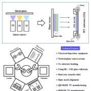
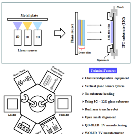
Hwang Chang-Hoon, CEO of OLEDON, which has developed plane-source deposition technology for small & medium-sized OLED and large area OLED, said that it is under development of vertical plane source deposition technology capable of manufacturing ultra-large OLED TVs of 77 inches or larger. Hwang introduced the related technology that it is possible to mass produce OLED TVs of 77 inches or more without the sagging problem of large substrate such as 12th generation (3300 x 4000 mm) substrate when using vertical plane source deposition technology.
According to Hwang, the production yield for 75 inch TVs or larger with the conventional inline type evaporator might be very low due to severe sagging of the substrate and difficult control of many linear sources. To solve this problem, Hwang said that a new 12-generation large-area cluster-type deposition technology is needed, and that vertical plane source deposition technology will be an appropriate alternative.
On the other hand, OLEDON holds the original patents for plane source deposition technology. It also filed a patent related to the curved plane source FMM deposition for high-resolution AMOLED manufacturing, and a patent related to the vertical plane source deposition technology for manufacturing large-area OLED TV.
OLEDON is a company which develops plane source deposition technology for high resolution AMOLED manufacturing. Hwang Chang-Hoon, CEO of OLEDON announced in IMID 2018 that it developed ‘curved plane source FMM deposition technology’ that can be adopted to 2250ppi AMOLED pixels, for the first time in the world.
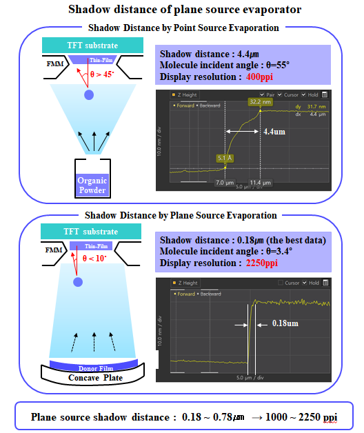
Conventional linear source FMM deposition technology has a shadow distance of 3um. The available production range is 570ppi AMOLED resolution. On the other hand, the plane source deposition technology already demonstrated in OLEDON can achieve a resolution of 800 to 1200 ppi of AMOLED with a shadow distance of 0.8 to 1.5 μm. Meanwhile, the newly developed ‘curved plane source FMM deposition technology’ is an upgraded technology of the plane source deposition technology which can realize the maximum resolution of AMOLED to 2250ppi with a shadow distance of 0.18 ~ 0.6μm.
The principle is that light is gathered through a concave mirror, a curved surface is applied to the conventional flat plane source, and the light emitting material does not spread, but is precisely deposited at a desired position, thereby reducing the shadow distance.
If this technology is commercialized, it is expected that it can be widely applied not only to mobile devices but also to virtual reality devices.
Various solutions for high resolution OLED implementation were released at iMiD 2017 held in COEX from October 18th to 19th. As the resolution of small and mid-sized OLEDs, which are currently being commercialized, is staying at the QHD level, the solutions released at this time have attracted a great deal of attention from display members.
First, Hwang Chang-hoon, CEO of OLEDON, who is developing plane source FMM deposition technology, announced at the business forum, “The plane source FMM deposition technology currently being developed is the only alternative for ultra-high resolution OLED manufacturing at 2,250 ppi”. Hwang Chang-hoon CEO said, “We measured the shadow distance using a-step, and it was 0.38 μm. We can fabricate OLED device with 2,250 ppi only if we have this shadow distance.” “We are currently looking for shadow-free process conditions”
<Difference in shadow distance between point source and plane source>
In addition, Hwang Chang-hoon said, “We first co-deposited the host material and the dopant material on the metal plate to evaporate the deposited green donor thin film and measure the green target thin film with the same PL wavelength for the first time” and “Color control of target thin films made with plate sources can be controlled by the amount of dopant molecules in the donor film, so color control is expected to be easy”.
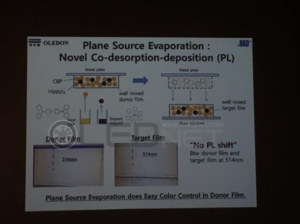
<OLEDON plane evaporation co-deposition material>
AP Systems, which recently announced the successful development of 1,000 ppi FMM using ultra-short pulse laser (USPL), exhibited 5.28 inch FMM of 825 ppi and 4.72 inch FMM of 677 ppi at this exhibition. A company official said, “By developing a burr-free laser process to solve the burr problem caused by the heat generated during the fabrication process, it is possible to fabricate not only FMM of 1170 ppi but also FMM of various shapes”.
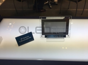
<5.28 inch 825ppi FMM of AP Systems>
Finally, Philoptics unveiled FMMs fabricated using electro forming, especially, FMM of 1,200 ppi, which attracted attention this time, was displayed separately in the VIP room. A company official said “We have secured the stability of the process for the production of 1,200 ppi FMM,” and mentioned “We plan to deliver it to panel makers for testing in the first half of next year, and aim to develop FMM at 2,000 ppi later.”
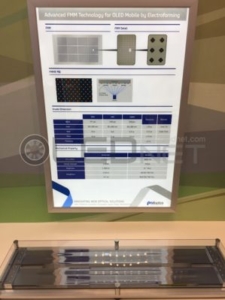
<FMM of Philoptics manufactured by electro forming method>
As such, in this iMiD 2017, various solutions for high-resolution patterning of OLEDs has been released. Recently, as the number of contents requiring high-resolution OLED such as virtual reality contents increases, interest of smartphone users are increasingly interested. It is worth noting which solution will enable the small to medium-sized UHD OLED era.
Recently VR contents experience through smart-phone device has been increased, therefore high resolution of smart phone is becoming necessary. However, OLED smart-phone resolution still remains at QHD level for 3 years since QHD OLED is applied to Galaxy Note 4 for the first time in 2014.
The core point that decides resolution of OLED smart-phone is evaporation process for emission layer. Bottom-up type evaporation method, which is applied to the recent devices is that substrate and FMM (fine metal mask) are horizontally arranged on the upper side of evaporator and vaporize the organic material from the lower linear source in order to form RGB layer.
Thin FMM measures less than 15um thick is necessary for making high resolution OLED like UHD level, however, as FMM gets thinner, it would be difficult to make mass production because technical problems will be occurred such as patterning, sealing and welding.
In order to solve these problems, various metal mask patterning technologies are being developed such as vertical type evaporation and plane source evaporation.
Vertical type evaporator that arranges board and FMM vertical is developed by Hitachi of Japan for the first time. And Canon Tokki exhibited Gen6 vertical type evaporator at Finetech Japan 2013, however it is not being used for mass production at the moment.
![]()
<Canon Tokki’s Gen6 vertical type evaporator which is exhibited at Finetech Japan 2013>
According to the recent ETNEWS, Applied Materials developed Gen6 flexible OLED vertical type evaporator and it is being tested in Japan Display.
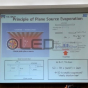
Plane source evaporator is being tested but also the linear source type. Plane source evaporator method is that an organic material is first evaporated on the metal surface to produce plane source, then re-evaporated in order to form an organic thin film on the substrate.
In the past iMiD 2017, representative of OLEDON, Chang Hoon Hwang mentioned that 2250 ppi resolution OLED can be implemented through plane source evaporator.
For metal mask patterning technology, electro forming and laser patterning technology is highlighted. Electro forming method is developed by Wave Electronics, TGO Technology, Athene and so on. Laser patterning technology is being developed by AP Systems.
As such, development for high resolution OLED is receiving great attention whether it can solve the current problems and contribute to UHD resolution implementation for OLED smart-phone.
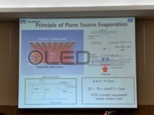
<Principle of plane source evaporation developed by OLEDON>
Three years have passed since the first QHD (about 515 ppi) OLED applied to Galaxy Note4 in 2014, but OLED resolution is still in QHD. In order to manufacture high-resolution OLED over UHD, FMM of less than 15 μm is required, but it is not applied to mass production due to various technical issues.
Professor Hwang Chang-Hoon, CEO of OLEDON, a venture business of Dankook University, proposed that the plane source FMM deposition technology is the only solution for a high-resolution OLED manufacturing process over UHD at the 1H semester UBI Research Seminar “OLED Market Analysis and Latest Technology” held on June 30 (Fri) at Yeouido FKI Conference Center.
Professor Hwang Chang-Hoon said, “To improve the resolution of AMOLED, the angle of flight of organic molecules should be reduced to less than 10 degrees and the aspect ratio of TFT devices should be maintained at 1.0 level.” and explained “The evaporation angle (incidence angle) of the currently known linear source is about 40 degrees, and the shadow distance is about 3 um. Therefore, the ratio of the pattern width, the shadow distance, and the aspect ratio can be increased at the SUHD level AMOLED patterning process. Ultimately, the current patterning technology loses the flatness of the film. “.
In addition, Professor Hwang Chang-Hoon said, “Linear deposition technology has limitations in achieving resolution higher than QHD, and development of plane source FMM deposition technology is the only way to manufacture OLED with 2000 ppi or higher.”.
![]()
<Professor Hwang Chang-Hoon announced the 2250ppi AMOLED technical problem, Source: the 1H semester UBI Research Seminar>
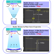
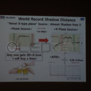
The shadow distance measured by OLEDON’s plane source FMM deposition technique ranges from 0.68 to 1.05 μm and the angle of incidence is 13 to 19 degrees and converting this result to resolution makes it possible to fabricate a device with a maximum of 1500 ppi. On the other hand, with the newly developed Xplane source, the shadow distance was 0.38 ~ 0.56um and the incident angle was 7.2 ~ 8.0 degrees, it is possible to manufacture up to 3300 ppi device by converting it to the resolution. In the last SID2017, Prof. Jin Byung-Doo and Prof. Hwang Chang-Hoon introduced the world’s first measurement of sub-micron-scale shadow distance using plane source patterning technology, it has been announced that it is possible to manufacture a micro AMOLED device having a Super Ultra (SUHD) resolution of 11K (2250 ppi) or more if scale-up development is applied to large-area OLED display production industry in the future. (Paper title: Plane source evaporation techniques for Super ultra high resolution flexible AMOLED)
![]()
Sub-micron Shadow data and incident angle data obtained by plane source FMM deposition technology, Source: the 1H semester UBI Research Seminar
On the other hand, based on the development results, OLEDON announced that it plans to develop and install planar source FMM evaporator for research, which can manufacture ultra-high resolution micro OLED devices using plane source deposition technology, in Dankook University. (Refer to: OLEDON homepage www.oledon.co.kr)