Merck Has Completed the Development of Organic Material Samples for Low Dielectric Constant TFE Below 2.5 [2022 Second Half OLED Seminar]
Touch of flexible OLED for smartphones is divided into add-on and on-cell. Add-on is a method in which a touch electrode is formed on the top of the film and the touch film is adhered to the top of the encapsulation layer through OCA.
On-cell is a method in which touch electrodes are created directly on the encapsulation layer, and is a mainstream technology applied to Samsung Electronics’ “Galaxy” series and Apple’s “iPhone” series.
The on-cell method reduces material costs because it creates electrodes directly without using films and OCA, while the absence of films and OCA shortens the distance between touch electrodes and TFT, increasing signal-to-noise (SNR).
")
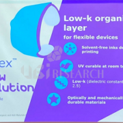
Merck, Low-K Organic Materials for TFE(Second half of 2022 OLED Seminar)
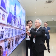
At the “2022 Second Half OLED Seminar” held at the FKI Hall in Yeouido on November 9, 2022, Merck announced that it is developing a low dielectric constant organic material for TFE to reduce SNR and is currently developing a 3.1 dielectric constant value for TFE to below 2.5.
Merck noted that blocking noise from TFTs is ultimately the role of organic matter, which occupies the thickest part of TFE, and revealed that it has developed a sample material available in the N2 environment.
Lastly, Merck concluded its presentation on organic materials for TFE, saying that the lower dielectric constant of organic materials can affect reliability due to lower membrane density, but that reliability has been secured in the Lab environment, and that they will secure reliability in mass production through cooperation with panel companies.
")
Merck, Low-K Organic Materials for TFE(Second half of 2022 OLED Seminar)
 2022 OLED Emitting Material Report Sample Download