Posts

LG Display 88-inch 8K OLED TV was released to the public through CITE held in Shenzhen, China

CITE, an electronics trade show held in China on April 10, 2018, had a relatively lukewarm atmosphere with significantly fewer visitors than last year. It seems to have been influenced by the lack of special IT issues, compared to last year when it was crowded with the attention of many general visitors.

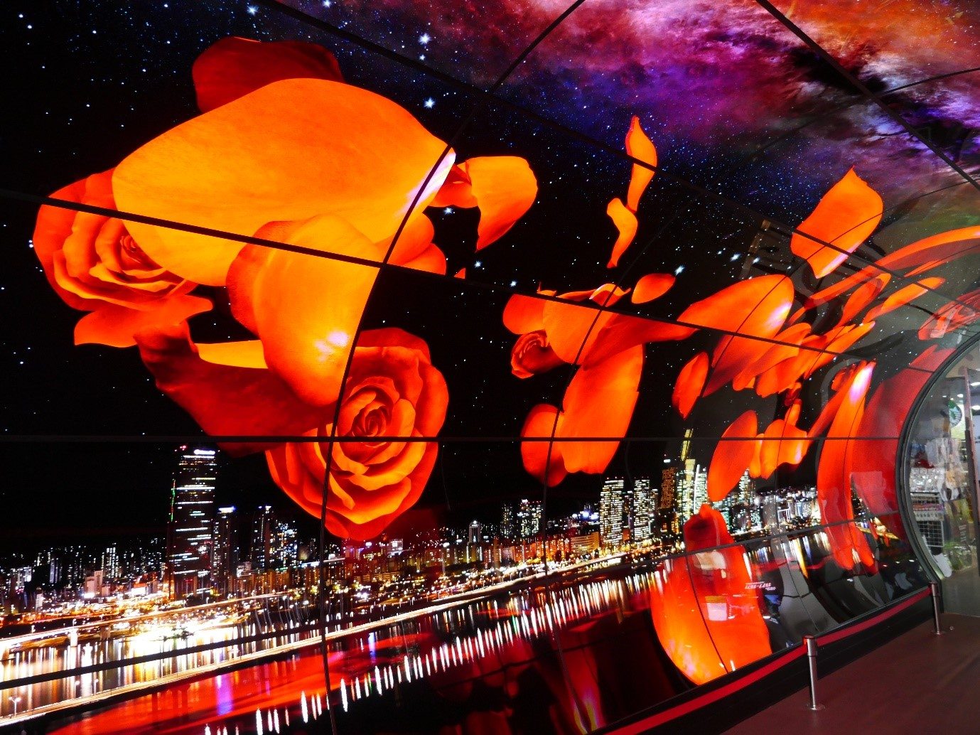
Especially, there were no new products on the TV appliance side. Most of the exhibitors displayed the same products as those of last year or 2018 CES. On the other hand, LG Display unveiled its 88-inch 8K OLED TV, which had been hiding in its own booth, at the front of the booth. CSOT also showcased OLED displays made with printing technology that had been publicized several times during several conferences. 8K OLED TV is to be the future of the high-end premium TV as it clearly shows the advantages of OLED display such as contrast ratio, sharp image quality and color reproduction through large screen. CSOT’s 31-inch display is meaningful because it exhibited the results of CSOT’s printing OLED technology development. It is preparing for a new investment of about 20K TV line next year. The exhibited product was manufactured by using top emission Ink-jet printing technology to oxide TFT. The peak brightness is 150 nit at 144 ppi.
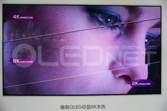
<88 inch 8K OLED TV – LG Display>
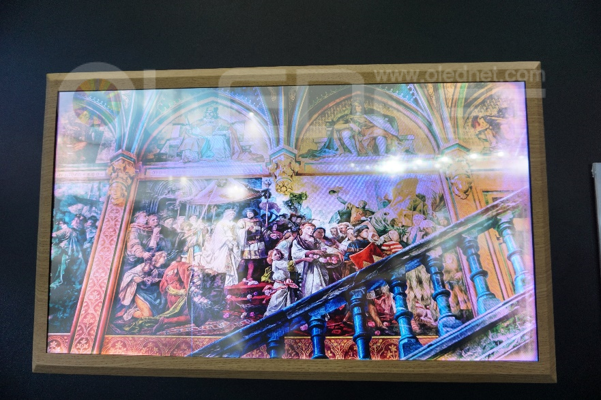
<31inch Ink-jet printed OLED Display – CSOT>

Vivo, which was the first to unveil the smart phone X21 with a built-in fingerprint sensor, displayed only the X21 model at its booth.  As a result of the actual registration testings, the fingerprint was recognized several times compared to the existing fingerprint registration, and the test recognition rate was not bad, but the response speed was slightly slower than opening the screen with the home button. In addition, most panel makers exhibited displays similar to the notch design of the iPhone X, which created various issues over the past six months, and set makers such as Vivo and Oppo released similar notch type smart phones. According to one official of some panel maker, the response to the design is not positive, but he said the company made it along with Apple. In his personal opinion, he preferred full screen design. Despite the sluggish performance of iPhone X, it still shows Apple’s strong market influence that the smart phones of the similar designs were released.

BOE, which started the operation of its Chengdu factory in 3Q 2017, exhibited various OLED panels made using plastic substrates. One official of BOE expressed confidence that it is only Samsung Display and BOE that can mass produce flexible OLED panels using plastic substrates across the globe.

QD-OLED TV, is it to be the next generation premium TV?

Samsung Electronics is currently occupying the premium TV market with QD-LCD TVs, which use ‘PL-QD (photoluminescence quantum dot) technology’. This technology has a mechanism in which the material stimulated by external light re-emits light.

The operating profit of the consumer electronics division (CE), which controls QD-LCD TVs, fell more than Korean won 1 trillion in last year and the operating profit ratio was only 3.6%.

On the other hand, LG Electronics’ HE business division achieved a record operating profit of Korean won 1,566.7 billion and an operating margin of 8.1% through OLED TV. Sony also turned its operating profit into a surplus by quickly taking over the premium TV market with OLED TV.

OLED TV has had a positive effect in driving corporate sales growth.

Samsung Electronics has been developing EL-QLED, with EL-QD (electroluminescence quantum dot) technology, to increase its market share in the premium TV market. However, efficacy, lifetime and mass production technology of quantum dot, which is the material of QLED, is not yet secured.

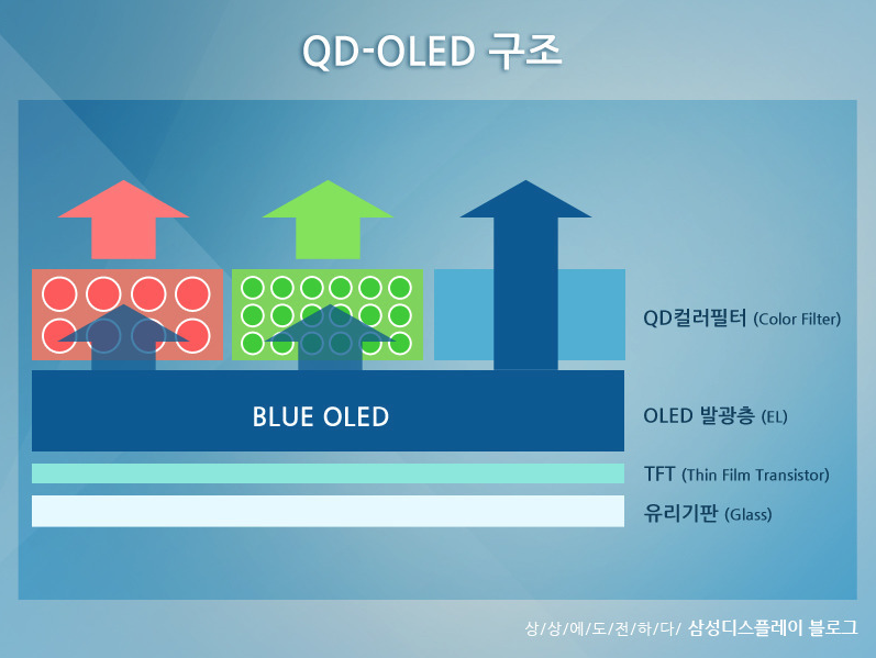
Recently, QD-OLED TV technology, which uses blue OLED as a light source and that implements red and green colors through a quantum dot color filter (QDCF), is attracting attention.

<Expected structure for QD-OLED, Source: Samsung Display Blog>

By using QDCF, it is possible to easily make desired colors by adjusting the size of the QD material and improve the color reproduction rate. This is because the color gamut is enlarged to BT2020, so it is close to natural color and it is possible to deliver vivid picture quality more clearly. In addition, QD-OLED TV has a top emission structure, which makes it easy to secure the aperture ratio, thereby improving resolution and screen uniformity.

However, in QD-OLED TV, there are various problems to be solved such as lifetime and efficiency of blue OLED, and technology of ink-jet printing process. Given that the industry is still in the early stages of reviewing the business possibility, QD-OLED TVs are expected to go into mass production after 2020.

Attention is focused on the QD-OLED TV’s entry into the premium TV market and its impact.

RGB ink-jet printing, also applied to small and medium-sized OLED?

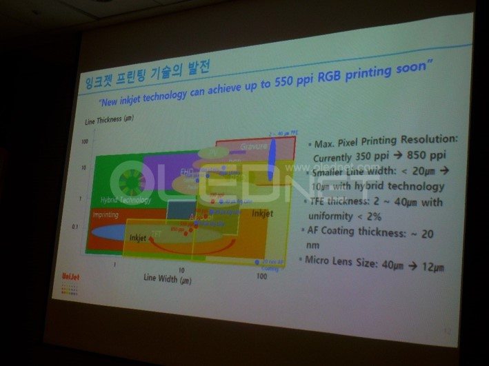
At the “Year End Seminar of OLED/Display” held at COEX in Seoul, Korea, on December 7, Kim, Seok-Soon, CEO of Unijet said that ink-jet printing technology can implement over 550 RGB ppi and ink-jet printing can be applied to small and medium-sized OLED process as well.

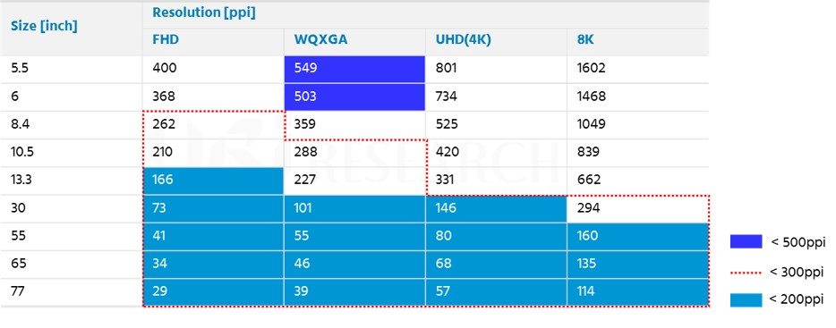
The currently mass-produced QHD resolution of 5.5-inch mobile device is 550 ppi but it is actually 400 ppi with pentile structure. Moreover the ink-jet printing technology for RGB pixels is currently in the range of 150 to 200 ppi which can achieve 8K resolution on over 55inch OLED, yet inapplicable to the small and medium-sized OLED process. As Kim announced, if the ink-jet printing technology is applicable, implementing 550 ppi in the small and medium-sized OLED process, beyond QHD resolution in 5.5 inches, it is possible to implement UHD resolution in pentile structure.

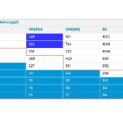
<ppi by size and resolution>

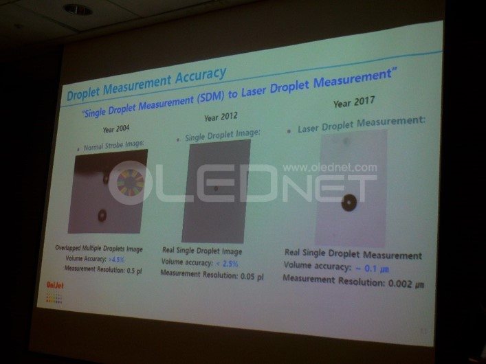
Kim said, “In 2012, single droplet measurement technology showed 2.5% or less of volume accuracy, which was, however, insufficient for RGB printing.  In 2017, the laser droplet measurement technology enabled the discharge volume control less than 0.1 μm and the real-time internal pressure control reduced the volume accuracy by less than 0.1%.” Kim added that it is possible to form over 550 RGB ppi regardless of the pixel structure.

Lastly, Kim noted that the solvent purity for OLED RGB pixel is very important; “Inkjet printer can be commercialized only if ink materials are fully developed first to satisfy panel makers. He expected that it will be applied to the mass production line in earnest since 2020. ”

Solution Process OLED, Max. 40% Decrease in Component Material Cost Possible Compared to WRGB

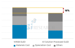
According to 2017 Solution Process OLED Annual Report published by UBI Research, when solution process (ink-jet printing) is applied to large area OLED, it could reduce up to 40% of component material cost, and approximately more than 18% of production cost compared to WRGB process that uses evaporation method.


Solution process is a technology that can manufacture RGB pixel structure of large size OLED panel without cutting mother glass using Gen8 manufacturing equipment or larger.


UBI Research analyst Hyunjun Jang explained that the solution process applied OLED has a simpler panel structure with 5 layers compared to 20 layers of WRGB OLED. WRGB OLED process material usage efficiency is only at 40% but solution process application could increase this to over 90%. Jang added that the lack of color filter is a factor that could decrease panel production price by reducing development cost. Particularly, this can greatly reduce emitting materials usage which occupies much of materials cost and contribute considerably to the fall in production cost. Furthermore, he added that cost setting of soluble emitting material per gram will be an important factor in production cost decrease and emphasized that organic material usage greatly decreases when soluble emitting materials are used but must consider price increase due to solvent cost, production cost, and development cost.


Solution process technology continues to receive attention as a key technology that can lead popularization of large area OLED, and key AMOLED panel companies are carrying out development.


In terms of technology, solution process OLED has lower emitting efficiency and short lifetime as diverse solvent is added to existing evaporation materials to transform into ink leading to low purity. This has been an important issue for panel and material companies for past several years. To improve this, DuPont, Merck, Sumitomo Chemical and others have been actively developing soluble OLED emitting materials. Much like evaporation materials, blue materials showed particular difficulty in performance improvement. However, at present significant portion of technology development has been carried out and investigation shows approximately 80% of lifetime and efficacy of has been achieved compared to evaporation materials.


2017 Solution Process OLED Annual Report compared and analysed WRGB OLED and solution process OLED’s competitiveness in terms of process, materials, and cost. Key issues, soluble OLED emitting materials development status, key companies’ trend, and solution process OLED market are analysed from various perspectives.

<Source: WRGB OLED and solution process OLED production cost comparison, UBI Research 2017 Solution Process OLED Annual Report>

Merck, introducing future-oriented material for the display in SID 2017

Merck said new display technologies and upcoming projects will be presented at SID Display Week 2017

In addition, Merck will exhibit a broad portfolio of products and services under the theme of ‘The Perfect Pixel – Advanced materials for display and beyond’.

“We are gradually improving not only display technologies but also quality, reliability and service through our close relationship with our clients,” said Michael Heckmeier, General Manager of Display Materials Business at Merck.

He also revealed the future plan, saying “continuous development will further solidify our market position as a leading company. We will provide a better product experience for end-user by developing eco-friendly and efficient production processes. ”

To this end, Merck added, “apart from unrestricted designing, flexibility, or color gamut, contrast and energy efficiency, we can focus on innovative products such as liquid crystal window (LCW) module.”

<OLED Display, source: Merck>

At the SID conference, Merck will present the development status of soluble materials for ink-jet printing.

According to Merck, red and green layers made with ink-jet printing have shown efficiency similar to those made with vacuum deposition technology.
Ink-jet printing approach can realize a large-sized OLED panel bigger than Gen8 with RGB pixel structure; it is developed as a simple layer with high material utilization efficiency, which is cost effective in mass production.

At the OLED Korea Conference, Merck said, “Red shows a 16.4% luminescence efficiency and LT95 2,000h long life expectancy; for green 18.7% and LT95 8,000h; blue 7.5% LT95 500h (based on 1,000cd/m2). He once said that the corporate goal is to develop a fluorescent blue dopant with  luminous efficiency higher than 11%, a phosphorescent deep red dopant improving from 20 cd/A brightness to 80 cd/A and phosphorescent green dopant with improved roll off.”

When 55inch OLED TV below US$ 1,000 will be realized?

At an analytical seminar on market entry potential of OLED and Solution Process OLED having been held in Small& Medium Business Center on October 14th, Manager Jeong Seong-jin of DuPont had time of introducing tendency regarding soluble OLED material and contents of the latest development.
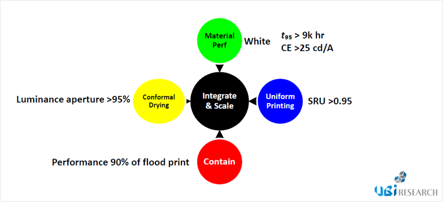
Manager Jeong said that soluble OLED material and processing technology were on the verge of completion, but problems about how to complete Solution Process by combining it was still remained as issues, and also stated that Material performance (T95>9k hr, CE>25 cd/A) and Uniform printing (SRU>0.95), Contain (performance 90% of flood print), Conformal Drying (luminance aperture>95%) would be key elements.

<4 key elements to make commercialization of Solution Process>

Dupont progressed R&D on Solution Process previously by utilizing Nozzle Printing method that used Surface Energy Modification. This method had merits such like controlling quantity was easy and the nozzle was not clogged up due to constant supply of solution, there were limitations according to panel material together with a lot of raw material consumption.
Dupont lighted up a fact that R&D has been progressed to the direction of deposing organic materials after forming Bank with Ink Jet Printing method owing to such problems and Ink Jet market having been enlarged recently, and then opened Ink Jet Material performance.
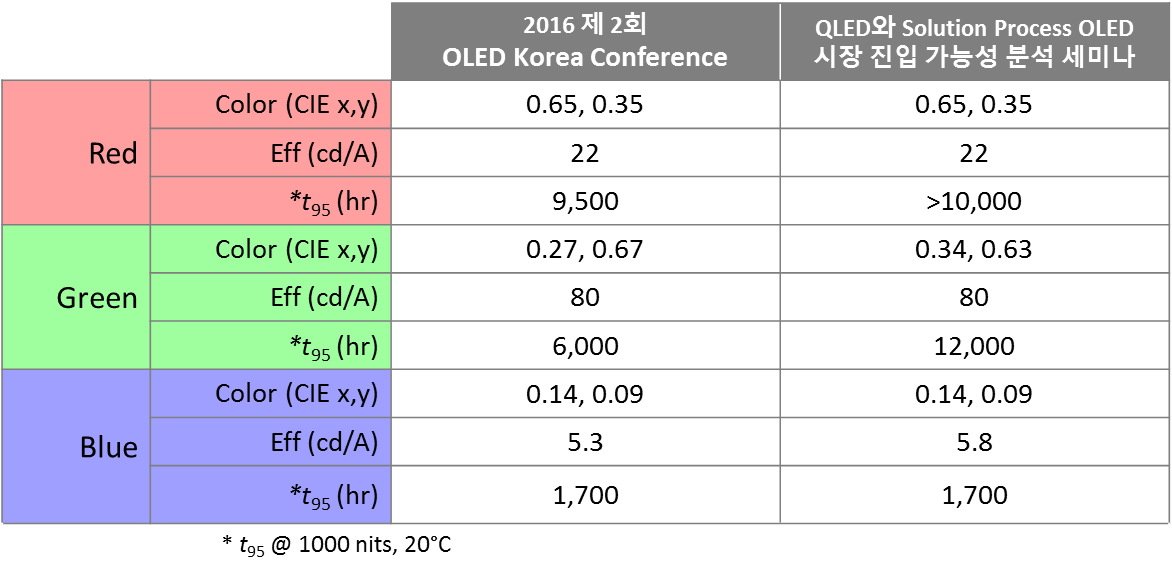
When comparing with datum pronounced in 2016 2nd OLED Korea Conference by Dupont, the life seems to be developed for Red and Green in priority, and efficiency for Blue. Approximately 6% of Red life and two times of Green were improved, and about 10% of Blue efficiency was turned out to be increased.
Manager Jeong Seong-jin put emphasis by saying “In order to expand market to OLED from display market having been enlarged gradually, adoption of Solution Process is essential, and concentration for developing soluble OLED luminescence material will be made so that 55inch OLED TV below US$ 1,000 could be produced massively until 2020 by using Solution Process in set makers.”

<Performance comparison with existing Ink Jet material of DuPont>