Posts

[28TH FINETECH JAPAN] JDI and JOLED, announced Strengthening Cooperation for Mid-sized OLED Market

At the 28th FINETECH JAPAN held in Tokyo, Japan from December 5 to 7, 2018, JDI and JOLED announced that they would intensify their cooperation in order to target the middle-sized OLED market.

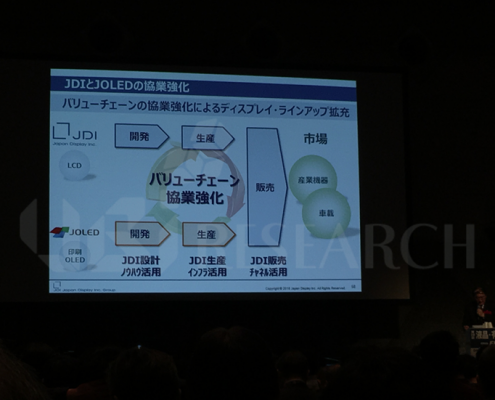
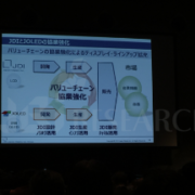
JDI announced that it will actively promote JOLED’s solution process OLED to medium-sized OLED markets such as industrial display markets or automotive display markets through its own design know-how, production infrastructure, and sales channels,.

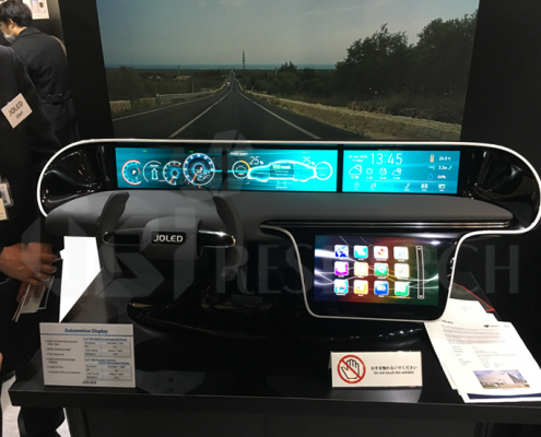
In particular, JDI announced that it will provide new value to next-generation automotive fields along with JOLED such as support for safety such as electronic mirrors and displays for A/B pillars, new interface functions, movie appreciation using 4-8K displays, and the displays that are harmonized with interior design such as curved surfaces and big screens.

JDI and JOLED also shared booths for exhibition. JOLED introduced 21.6-inch FHD OLED monitors for e-sports and medical applications. In addition, it introduced a number of medium-sized OLEDs such as 12.3-inch HD OLED for automobiles, 12.2-inch FHD flexible OLED, 27-inch 4K OLED for home interior, and 21.6-inch 4K flexible OLED with cylindrical form. It also showcased large OLEDs such as 54.6 inch 4K OLED.

On the other hand, JOLED announced in July, 2018 that it would open its Nomi office for mass production of solution process OLED. Based on 5.5 generation glass substrates, Nomi has production capacity of 20,000 glass substrates per month and plans to mass-produce in 2020.

JOLED raised 47 billion yen to spur solution process OLED business for automobiles.

JOLED, the world’s first to successfully commercialize solution process OLED products, announced that it had raised a total of 47 billion yen as a third-party capital increase.

According to JOLED, Denso will invest 30 billion yen, Toyota Tsusho 10 billion yen, Sumitomo chemical 5 billion yen and SCREEN Finetech Solutions 2 billion yen. JOLED is known to cooperate with Denso to develop automotive displays and Sumitomo chemical to develop OLED materials for solution process.

In particular, Denso has been mainly using TFT-LCD for automotive displays, but it is expected to lead the development for applying lightweight and easy-to-shape OLED to automobile interior through this investment.

It is expected that this funding will accelerate the establishment of production system for the mass-production of JOLED’s solution process OLED. JOLED announced on July 1 that it would set up a “JOLED Nomi Office” in Nomi-city, Ishikawa, and aim to operate in 2020.

Major production products are medium-sized (10 to 32-inch) solution process OLEDs that will be used for cars or high-end monitors. Also, Toshiaki Arai, chief technologist of JOLED announced that they would target the middle-sized OLED market with solution process OLED, at the 2018 OLED Korea conference hosted by UBI Research in March.


TCL announced “Establishing large-area OLED panel production plant”, is solution processed RGB OLED mass production accelerated?

China TCL will invest RMB 42.8 billion (US$ 6.71 billion) in Shenzhen to establish a factory for large-area OLED panel production. According to South China Morning Post, TCL recently announced that it will produce 90,000 units on the basis of 70-inch panel in the new production line of Gen 11 (3370 mm x 2940 mm) with the goal of mass production in March 2021 in the data submitted to the Shenzhen Stock Exchange. The main products are to be known as 65-inch and 75-inch OLED panels, and 65-inch, 70-inch and 75-inch display panels with 8K resolution.

TCL will form a partnership with the China Development Fund for the necessary financing and will set up a new production line at TCL’s semiconductor subsidiary with RMB 20.3 billion.

Large-area OLED to be produced by TCL is expected to adopt solution process RGB. At the ‘4th OLED Korea conference’ hosted by UBI Research in March, James Lee, deputy chief engineer of TCL mentioned about the development of next-generation premium TV with the screen size of 70-inch or more and 8K resolution, based on the solution process.

Lee said, “The price difference between OLED TV and premium LCD TV is estimated to be reduced to 1.4 times when the price of large-area OLED panel is lowered by the operation of LG Display’s Gen 10.5 plant in 2020. We are developing solution process technology for large area OLED and it will be applicable to Gen11 factory. ”

Gen 11 production line is capable of producing six sheets of 75-inch OLED panels, being able to achieve a yield three times higher than Gen 8.5 production line and a cutting efficiency of over 95%. In addition, it is possible to produce large-area OLED panels with a real RGB structure instead of the WRGB structure when solution process is applied. Based on this, TCL emphasized that the construction of the Gen 11 solution process OLED mass production line is essential. Meanwhile, TCL has jointly established JUHUA Printing Display Technology with Tianma, a Chinese company, in 2016 through CSOT, which is a subsidiary of TCL, and is continuously developing the inkjet printing process by a Gen 4.5 R&D pilot plant.


Solution Process OLED, Max. 40% Decrease in Component Material Cost Possible Compared to WRGB

According to 2017 Solution Process OLED Annual Report published by UBI Research, when solution process (ink-jet printing) is applied to large area OLED, it could reduce up to 40% of component material cost, and approximately more than 18% of production cost compared to WRGB process that uses evaporation method.


Solution process is a technology that can manufacture RGB pixel structure of large size OLED panel without cutting mother glass using Gen8 manufacturing equipment or larger.


UBI Research analyst Hyunjun Jang explained that the solution process applied OLED has a simpler panel structure with 5 layers compared to 20 layers of WRGB OLED. WRGB OLED process material usage efficiency is only at 40% but solution process application could increase this to over 90%. Jang added that the lack of color filter is a factor that could decrease panel production price by reducing development cost. Particularly, this can greatly reduce emitting materials usage which occupies much of materials cost and contribute considerably to the fall in production cost. Furthermore, he added that cost setting of soluble emitting material per gram will be an important factor in production cost decrease and emphasized that organic material usage greatly decreases when soluble emitting materials are used but must consider price increase due to solvent cost, production cost, and development cost.


Solution process technology continues to receive attention as a key technology that can lead popularization of large area OLED, and key AMOLED panel companies are carrying out development.


In terms of technology, solution process OLED has lower emitting efficiency and short lifetime as diverse solvent is added to existing evaporation materials to transform into ink leading to low purity. This has been an important issue for panel and material companies for past several years. To improve this, DuPont, Merck, Sumitomo Chemical and others have been actively developing soluble OLED emitting materials. Much like evaporation materials, blue materials showed particular difficulty in performance improvement. However, at present significant portion of technology development has been carried out and investigation shows approximately 80% of lifetime and efficacy of has been achieved compared to evaporation materials.


2017 Solution Process OLED Annual Report compared and analysed WRGB OLED and solution process OLED’s competitiveness in terms of process, materials, and cost. Key issues, soluble OLED emitting materials development status, key companies’ trend, and solution process OLED market are analysed from various perspectives.

<Source: WRGB OLED and solution process OLED production cost comparison, UBI Research 2017 Solution Process OLED Annual Report>

What is the future of OLED?

Choong Hoon Yi, president of UBI Research made a keynote speech with a theme “The Future of OLED” at ‘The 3rd OLED Korea Conference’ hosted by UBI Research for two days from March 8 to 9.

Choong Hoon Yi, president of UBI Research stated “100-inch rollable wall TV is the future of OLED”. “human eyes have a wide viewing angle so even if display covers the whole wall, there is no discomfort. Glass substrate OLED may be difficult to carry, and accordingly rollable display can be rolled up and delivered like a carpet.” he added.

He also predicted “plastic substrates and printing process for price cut will be suitable for rollable display. TFT and pixel production techniques made by Solution process will be a key to future technology”. If a speaker is built in rollable display, and a correspondence between the person and sound on the screen will represent a perfect display.

Choong Hoon Yi said the reasons for the success of OLED can be found out in the mobile market.
Firstly, 4K contents to be used for future TVs will be used in smartphones, and smartphones will also use 4K resolution.

Second, Apple will release the OLED iPhone this year, and there will be an Apple effect because Samsung Display is building the A3 line for Apple to produce 200 million 5.5-inch OLED displays.

Third, Chinese market accounts for 40% of the global smartphone market, and Chinese set companies have been rapidly increasing the release of smartphones.

Lastly, a flexible OLED to cover the full screen smartphone will have no home button and feature wide screen to satisfy visual functions, and its strengthened security system that reads fingerprint and pattern can be applied.

For the four reasons above, he expected OLED will be key in the future mobile market.

Meanwhile, he expected the shipments of OLED panel will be 1.7 billion in 2021, and the sales will amount to US$ 75 billion. Korean display companies will represent more than 80% of the total market in 2021, and China will take up 10~15%. In addition, he forecast that display panel companies will make a new investment in flexible OLED which will account for 70% of the total OLED market.

UDC Introduced Organic Vapor Jet Printing That Keeps the Life time and Efficiency of OLED Emitting Material

Mike Hack, vice president of UDC introduced solution process technology, OVJP (Organic Vapor Jet Printing) technology during the COLOR IS UNIVERSAL Session of “The 3rd OLED KOREA CONFERENCE” hosted by UBI Research.

Mike Hack emphasized “OVJP technology can still use OLED materials used for the deposition process unlike the existing ink-jet solution process, and FMM and solvent are unnecessary”.

Besides, he introduced UDC’s Novel BY Display Architecture. According to his announcement, this structure has increased the mask opening size for one-time 2 pixel deposition. Also, Novel BY Display Architecture features the alternate deposition of blue and yellow sub pixels instead of existing RGB, and red and green CF in half of yellow sub pixel is arranged in a vertical symmetrical fashion.

Mike Hack said “This structure maximized not only the fill factor of blue and yellow sub pixel but also the color reproduction rate, efficiency and life time of OLED panel”. He also mentioned it can reduce manufacturing costs due to the use of less than 3data per pixel and 2-step EML deposition(FMM).
Lastly, UDC closed its announcement adding that they aim at the development and commercialization of PH emitter and host.

Meanwhile, according to “Market Entry Analysis for Solution Process OLED” by UBI Research, the emitting material used for the ink-jet solution process employs a method of mixing various solvents in an emitting material used for the deposition process. It lowered the purity of a materials, thereby reducing emitting efficiency and life time. Despite this advantage, solution process can increase the usage efficiency of emitting materials without using color filter and manufacture large-screen OLED panels via RGB pixel structure without panel split through over Gen8 equipment. Due to this advantage, major panel companies are actively developing it and trying to achieve the preoccupancy of commercialization.

Solution Process OLED TV is prospected to be launched on the market in 2019, targeting the Mid-end TV Market

According to “Market Entry Analysis for Solution Process OLED -The Possibilities and Opportunities” issued on November 14 by Ubiresearch, OLED TV, produced in solution process method, is prospected to be launched on the market in 2019.

Solution process is a technology which enables producing OLED panel in RGB pixel structure without any panel division on a device higher than G8, which major AMOLED panel producers has actively engaged in developing.

However, lamp efficiency and life cycle have no option to decrease because luminescent materials have lower purity than that of evaporation materials as luminescent materials applied to solution process should be mixed with various solvents in order to make the existing evaporation materials ink. Nevertheless, why major panel producers has actively engaged in developing solution process is that production cost can be declined as the usage efficiency of luminescent materials is high without using color filters and its structure is simpler than that of OLED panel using WRGB method.

According to the report, it is said that although developing luminescent materials for solution process OLED has been fully engaged, it should be more efficient than that of WRGB methods so as to enter the premium market. However, it seems substantially difficult that the capacity of solution process OLED surpasses that of WRGB as WRGB has been developed in top emission structure to improve its efficiency by over 20% and evaporation materials have also constantly been developed. Rather, based on proper level of life cycle and efficiency, it would be competitive to replace LCD targeting the mid-end TV market, according to the report.

Issues on OLED, QLED, hybrid QD, which can be applied to solution process and possibilities to enter the market, comparative analysis on the capacity of present solution process OLED, supply chain of QD industries, and major soluble OLED material producers are included in this “Market Entry Analysis for Solution Process OLED -The Possibilities and Opportunities” and it is expected to help the relevant producers understand the solution process industry.

Meanwhile, it is predicted that the market of large-scaled solution process OLED panel over 55 inch will begin in earnest being mass-produced as of 2019 and have accounted for the entire wide OLED panel market by approximately 15% growing by approximately US$ 1,000 million by 2021.

When 55inch OLED TV below US$ 1,000 will be realized?

At an analytical seminar on market entry potential of OLED and Solution Process OLED having been held in Small& Medium Business Center on October 14th, Manager Jeong Seong-jin of DuPont had time of introducing tendency regarding soluble OLED material and contents of the latest development.
Manager Jeong said that soluble OLED material and processing technology were on the verge of completion, but problems about how to complete Solution Process by combining it was still remained as issues, and also stated that Material performance (T95>9k hr, CE>25 cd/A) and Uniform printing (SRU>0.95), Contain (performance 90% of flood print), Conformal Drying (luminance aperture>95%) would be key elements.

<4 key elements to make commercialization of Solution Process>

Dupont progressed R&D on Solution Process previously by utilizing Nozzle Printing method that used Surface Energy Modification. This method had merits such like controlling quantity was easy and the nozzle was not clogged up due to constant supply of solution, there were limitations according to panel material together with a lot of raw material consumption.
Dupont lighted up a fact that R&D has been progressed to the direction of deposing organic materials after forming Bank with Ink Jet Printing method owing to such problems and Ink Jet market having been enlarged recently, and then opened Ink Jet Material performance.
When comparing with datum pronounced in 2016 2nd OLED Korea Conference by Dupont, the life seems to be developed for Red and Green in priority, and efficiency for Blue. Approximately 6% of Red life and two times of Green were improved, and about 10% of Blue efficiency was turned out to be increased.
Manager Jeong Seong-jin put emphasis by saying “In order to expand market to OLED from display market having been enlarged gradually, adoption of Solution Process is essential, and concentration for developing soluble OLED luminescence material will be made so that 55inch OLED TV below US$ 1,000 could be produced massively until 2020 by using Solution Process in set makers.”

<Performance comparison with existing Ink Jet material of DuPont>

WOLED will lead premium TV market after 2020

UBi RESEARCH held ‘An Analytical Seminar on OLED Market Entry Feasibility of QLED and Solution Process’ on the 14th at Seoul Small& Medium Business Center.

CEO Lee Chung-hoon of UBi REARCH said “OLEd TV will show 16.7% market share in 2016 at the world premium TV market, and lead premium TV market with 68.1% share in 2020.” and analyzed such like “LCD TV could not follow OLED TV performance excluding low price and high solution.”

China is threating domestic LCD market in current wide TV market while displaying material superiority to LCD industry, and cost-effective rate of the wide TV is losing ground to Chinese products too. Thus, LG Display and LG Electronics did successful market entry after having equipped with competiveness in the premium market through OLED TV, and they are expediting mass-production investment and technical development aiming at dominating and popularizing premium TV market.

The most important factor in popularizing OLED TV is price. ASP (average sales price) of UHD OLED panel based on second quarter of 2016 is USD 720, and FHD OLED panel is approximately USD 450. It was expected that UHD OLED panel could lead TV market if it secured about USD 500.

Development to adopt solution process methods has been progressed in order to lower price of wide OLED panel in the industry, and QLED technology as an alternative of OLED TV is becoming an issue nowadays.

In relation with this, CEO Lee Chung-hoon forecasted like “As much as being closed to commercialization due to development of solution process OLED or QLED technology, WOLED technology becomes to be developed one step more, so market entry of solution process OLED and QLED will not be achieved easily. Specially, there are many technical issues in QLED which is considered as next OLED by Samsung Electronics, and 10 years of research will be required further.”

Also, he emphasized that the technology of being able to reduce cost vs. WOLED such as lessening layer numbers dramatically etc. should be developed in order to enter solution process OLED and market successfully, and the entry shall be made by targeting low-end market. In particular, he analyzed that WOLED would lead premium TV, and solution process QLED and QLED occupy the low-end market after 2020.

<TV Market Scenario after 2025 (Source: UBi RESEARCH)>

CYNORA Achieves a New Milestone in Efficiency and Stability of Blue TADF Emitters for OLEDs

CYNORA, a leader in TADF (thermally activated delayed fluorescence) materials, has developed new material classes that combine both, high efficiency and long lifetime, for blue emission. With these new achievements, the company is on track to reach the performance requested by the OLED industry. The commercialization of CYNORA´s TADF materials is therefore still planned for the end of 2017.

Earlier this year, in May 2016, CYNORA had established two blue emitter systems where one of them showed a high efficiency while the other showed a long lifetime. During the last 6 months CYNORA has made further, significant progress by combining high efficiency and long lifetime in a single blue emitter system. In an OLED device, the new blue material reaches 14% EQE (external quantum efficiency) together with a lifetime of 420h (LT80, at 500 cd/m2, λ < 480 nm). With this performance, CYNORA has now shown that blue TADF emitters can reach OLED display specifications soon.

“Our constant progress on blue TADF emitters was made possible by our growing team of TADF experts and by the close collaboration with CYNORA’s customers” says Thomas Baumann, CSO at CYNORA, “We have developed several classes of high performance TADF materials which we are currently optimizing for market readiness at the end of next year.”

CYNORA’s dopants are fully organic and designed for existing vacuum deposition. The company will adapt the blue TADF emitters for solution processing in a second step. With its blue TADF technology CYNORA will enable device makers to provide OLED displays with significantly increased energy efficiency and higher display resolution.

Possibility for market entry of Solution process OLED and QLED with new technology of large surface.

Currently in the market of premium TV, OLED TV and QD- LCD industries are highly competitive.

QD vision with Nanosis and SID 2016 and IFA 2016 also emphasized quality of TV with QD material included comparing quality of OLED TV. Against this, LG Display joined the completion by emphasizing quality of OLED TV as an ideal display for HDR with comparison between QD-LCD and OLED in IFA 2016 with from SID 2016,

In current large surfaced TV market, LCD TV is taking overwhelmingly large share in distributed market while OLED TV gradually is growing large share in premium market.

In looking into strategies of each industry, large surfaced OLED is developing solution process OLED in order to achieve broader market share with from premium model to distributed model. To overcome weakness compared to OLED, LCD TV industry progressively use QD material with the final goal of development of QLED technology

As a competition in premium TV market gradually extends to entire area of TV market, present condition and possibility of market entry with solution process OLED and QLED is one of major interest.

For this matter, there is seminar host by Ubi Industrial Research with the theme of “analysis in possibility of market entry with QLED and Solution process OLED” in Medium sized business center, Yeouido, October 14th and will be discussing present market industry of large surfaced TV and panel and also will be dealing with present condition and issue of QLED and Solution process OLED, and future possibility of market entry.

Choong-Hoon Lee, president of Ubi Industrial Research, will suggest future direction of OLED industry with analysis of present condition and possibility of market entry in OLED and QLED.

Sung-Jin Jung, head of department of Du Pont, will be discussing the timing of market entry of solution process OLED with the demonstration of soluble OLED material, the essential part of solution process OLED, including present trend and up to date developmental technique

Professor Chang-Hee Lee and senior researcher Ji-won Bang from Korean Institute of Ceramic Engineering and Technology(KICET) will be discussing about advantage and developmental issue of Quantum dot material and direction of future development.

The seminar attracts attention in terms of providing an opportunity to share and discuss regarding issue through media and exhibition with technological and market perspectives of Ubi Industrial Research and share opinions and future possibility.

For registration and any inquiry, please contact to Hana Oh (hanaoh@ubiresearch.co.kr, 02 577 4940) from Ubi Industrial Research.

[Lighting Japan 2016] What is the Key Issue of Solution OLED Materials?

In Lighting Japan 2016 (January 13-16) conference, Sumitomo Chemical and Merck revealed recently developed soluble OLED materials performance results.


The soluble OLED materials efficiency published in this conference reached ≥ 65% of UDC’s evaporation materials; particularly, Sumitomo Chemical’s red achieved ≥ 85%, and green reached ≥ 88% of UDC’s evaporation materials efficiency. Lifetime (LT 95) results were not as good as efficiency with red’s 25% and green’s approximately 40% (average).


Sumitomo Chemical and Merck both revealed that although in terms of efficiency the soluble materials almost caught up to evaporation materials, but lifetime requires further development.


Solution process is a method that allows for large area OLED panel production in RGB method using ≥ Gen8 manufacturing equipment. Key panel companies are actively carrying out research development, and the performance of soluble OLED material is considered the biggest issue. According to Solution Process OLED Report 2015, published by UBI Research, when solution process is applied the material cost can be approximately 40% reduced compared to the current evaporation process using large area OLED panel. The timing for the solution process application to mass production is expected to be decided depending on the development speed of soluble OLED materials.


OLED Materials Performance Comparison

OLED Materials Performance Comparison

UBI Research Organizes ‘2015 Display Printed Electronics Seminar’

The Opportunity to Understand Printed Electronics Technology

For That Competitive Edge in Global Display Industry


At present there is an intense competition within display industry between countries such as China with aggressive investment, and Japan that is looking for a comeback. For Korea to possess that competitive edge in display industry, a seminar is being prepared. This seminar will provide the opportunity to learn about printed electronics technology that is becoming a key technology and understand latest technology trend.


UBI Research (http://www.ubiresearch.co.kr, President: Dr. Choong Hoon Yi), an OLED specializing company, announced that the 2015 Display Printed Electronics Seminar will be held on October 7. This seminar will take place at The K Seoul Hotel in Seocho-gu in Seoul with a group of key experts who will discuss latest technology development trend in display based on printed electronics.


Printing process or solution process is a new production technology that is the center of much expectation around the world. Dr. Kyung-Tae Kang, the head of printed electronics center of Korea Institute of Industrial Technology, will examine the current printed electronics industry and propose its future. Dr. Kang is also a secretary for IEC TC119 which was established to respond to the printed electronics industrialization.


At this seminar, Professor Yongtaek Hong of Seoul National University will explain technological issues that need to be considered when producing ultra-thin transistor device using printed electronics technology. The printed electronics technology is receiving much attention as it can be applied to flexible elastic substrate, and low temperature process through large area is possible.


Dongguk University’s Professor Yong-Young Noh will give a presentation on printed electronics technology’s development trend and research content for flexible display development.


Also, Dankook University’s Professor Byung Doo Chin will discuss OLED RGB printing technology trend review for efficiency and stability improvement of small molecule and polymer OLED device by solution process, and high resolution OLED technology that can be actualized through inkjet printing. This OLED RGB printing technology based on printing process is a subject of active research as a replacement for the current vacuum thermal evaporation; pixel formation is difficult for large area through this evaporation technique.


Furthermore, essential topics on printed electronics are covered by industry’s top experts.

  • Technology Trend for Solution Process OLED Material (Dr. Jae-Min Lee, Korea Research Institute of Chemical Technology)
  • Technology Trend for Electrode Material and Process for Printing (Dr. chan-Jae Lee, Korea Electronics Technology Institute)
  • Blanket Application for Printed Electronics and Development Status (Dr. Noh-min Kwak, RPE Corporation)
  • Printed Electronics R2R Equipment Technology Status


UBI Research will bring together top quality industry experts as speakers toward Korea’s leadership in display industry and host a place of networking where industry-academic professionals can meet. UBI Research seminars, previously held twice a year, will become a monthly event.


Seminar attendance application can be made through the UBI Research homepage (www.ubiresearch.co.kr).