Posts

Is there possibility of High resolution(UHD) OLED Smart-phone generation?

Recently VR contents experience through smart-phone device has been increased, therefore high resolution of smart phone is becoming necessary. However, OLED smart-phone resolution still remains at QHD level for 3 years since QHD OLED is applied to Galaxy Note 4 for the first time in 2014.

The core point that decides resolution of OLED smart-phone is evaporation process for emission layer. Bottom-up type evaporation method, which is applied to the recent devices is that substrate and FMM (fine metal mask) are horizontally arranged on the upper side of evaporator and vaporize the organic material from the lower linear source in order to form RGB layer.

Thin FMM measures less than 15um thick is necessary for making high resolution OLED like UHD level, however, as FMM gets thinner, it would be difficult to make mass production because technical problems will be occurred such as patterning, sealing and welding.

In order to solve these problems, various metal mask patterning technologies are being developed such as vertical type evaporation and plane source evaporation.

Vertical type evaporator that arranges board and FMM vertical is developed by Hitachi of Japan for the first time. And Canon Tokki exhibited Gen6 vertical type evaporator at Finetech Japan 2013, however it is not being used for mass production at the moment.
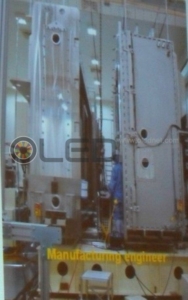
<Canon Tokki’s Gen6 vertical type evaporator which is exhibited at Finetech Japan 2013>

According to the recent ETNEWS, Applied Materials developed Gen6 flexible OLED vertical type evaporator and it is being tested in Japan Display.

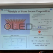
Plane source evaporator is being tested but also the linear source type. Plane source evaporator method is that an organic material is first evaporated on the metal surface to produce plane source, then re-evaporated in order to form an organic thin film on the substrate.

In the past iMiD 2017, representative of OLEDON, Chang Hoon Hwang mentioned that 2250 ppi resolution OLED can be implemented through plane source evaporator.

For metal mask patterning technology, electro forming and laser patterning technology is highlighted. Electro forming method is developed by Wave Electronics, TGO Technology, Athene and so on. Laser patterning technology is being developed by AP Systems.

As such, development for high resolution OLED is receiving great attention whether it can solve the current problems and contribute to UHD resolution implementation for OLED smart-phone.
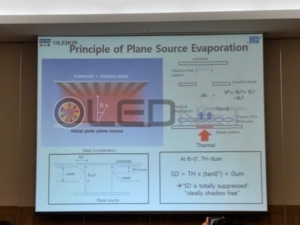
<Principle of plane source evaporation developed by OLEDON>

[iMiD 2017] AP Systems, Find FMM answers through USPL

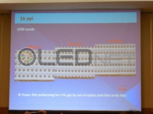
At iMiD 2017 in BEXCO, Busan on 28th, AP Systems announced that it succeeded in developing 1000ppi FMM with USPL (ultra-short pulse laser).

Since FMM plays a role of depositing pixels and RGB organic materials, FMM serves as a factor that determines resolution and yield of OLED. At present, FMM is mainly manufactured by etching method. This method has a problem that a shadow phenomenon due to the precision, thickness, and weight of the fine pattern occurs, in order to solve this problem, various FMM manufacturing processes such as laser processing and electro-forming have been developed.

Among these, laser processing method has an issue of forming burrs around pin-holes due to the thermal effect caused by laser irradiation. These burrs increase the shadow interval of the FMM, which causes overlapping of patterns during RGB organic deposition, thereby degrading the resolution of the OLED.

AP Systems has developed a burr-free laser process that does not have burr phenomenon and further controls the taper angle.

The Burr-free laser process is a short-time irradiation of unidirectional pulses at a constant number of times, since the laser is not continuously irradiated, it minimizes accumulated heat energy and prevents burr formation. In addition, by controlling energy of the laser, it accumulates energy and forms taper.

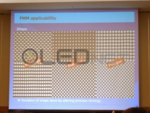
In this way, AP Systems explained ‘they produced FMM with various shapes of fine pin-holes such as square, diamond, and polygonal shapes, as well as 1170ppi FMM’, and ‘’We also developed large-area FMM manufacturing equipment with USPL method’.

AP Systems also added ‘multi-beam and USPL is equipped for FMM manufacturing equipment so that it can improve productivity and realize UHD’.

Since the launch of the Galaxy Note4 in 2014, the OLED resolution has remained at the QHD level yet. In order to manufacture an OLED having a high resolution (UHD level or higher), it is necessary to solve various technical problems faced by FMM. Accordingly, it is noteworthy how USPL technology of AP Systems will affect the future OLED market.

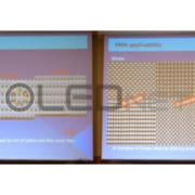
<1000ppi FMM produced by AP Systems>

<various type of FMM produced by AP Systems>

Developing ultra-definition display with a color filter technology

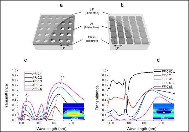
A color filter technology has been developed that can bring forward commercialization of next generation’s TVs with ultra-definition visibility and lower prices. The National Research Foundation of Korea (a chairman of the board, Moo-jae, Cho) announced that Prof. for Korea University, Byeong-kwon, Joo’s research team has developed a complementary plasmon color filter having sharp display and high resolution. The color filters which are currently used in the display industry mainly are optical absorption type using pigments or dyes. It has low chemical stability since it is based on organic materials and high unit cost due to manufacturing RGB filters separately. On the other hand, the optical interference type plasmon color filter using inorganic materials can simultaneously produce various color filters at low cost, but there is a problem that the color purity is in decline due to color interference occurring in the two-dimension array of nanostructures.

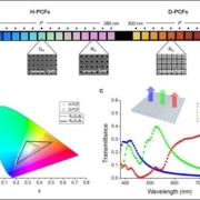
<Transmittance spectrum according to opening ratio of Hole pattern and dot pattern structures, Source: The National Research Foundation of Korea>

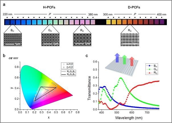
The research team applied a reversal approach to break out the existing pattern as complementary design method that combines dot pattern with hole pattern. It is a general viewpoint of academia that it is difficult to apply dot pattern to a transmission color filter in the form of reversing the existing hole pattern. However, the team assured that the extraction of high purity for red is possible through effective blocking the leakage of short wavelengths by dot pattern under certain conditions. The result is shown that the range of implementing color in the complementary designed plasmon color filter is widened over 30% than before.

<Plasmonic color filter of Hole pattern and Dot pattern structure produced, Source: The National Research Foundation of Korea>

In addition, the implementing of various color of the complementary plasmon color filters is available such as red, green, and blue by adjusting only the geometric parameters of the nanopattern. The performance can be improved without additional costs since the existing materials and manufacturing methods could be used as usual.

Prof. Byeong-kwon, Joo explained that “This research has developed a plasmon color filter with high color reproducibility through a complementary design method. This is expected to accelerate the development of the next-generation display combining nano-optic devices.”

The research results were performed by supporting of the Basic Research Support Project(private research) of the National Research Foundation of Korea at the Ministry of Science, ICT and Future Planning, the Ministry of Education·BK21 support project of the National Research Foundation. It was published in the Scientific Reports affiliated journal of an international journal Nature, on January, 13th.

[IFA2016] Where Does the Confidence of LG Electronics Come From?

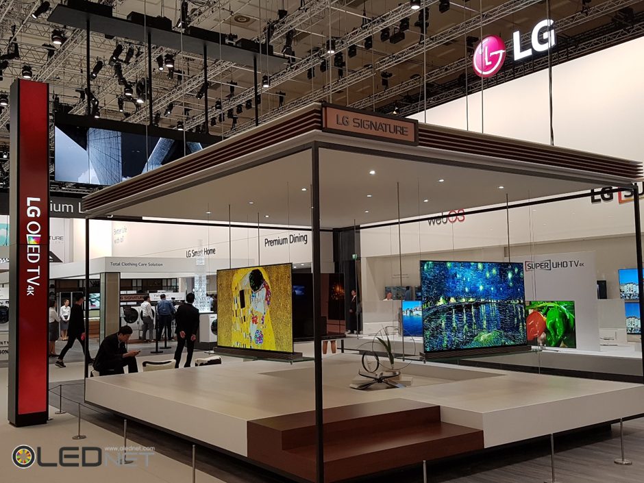
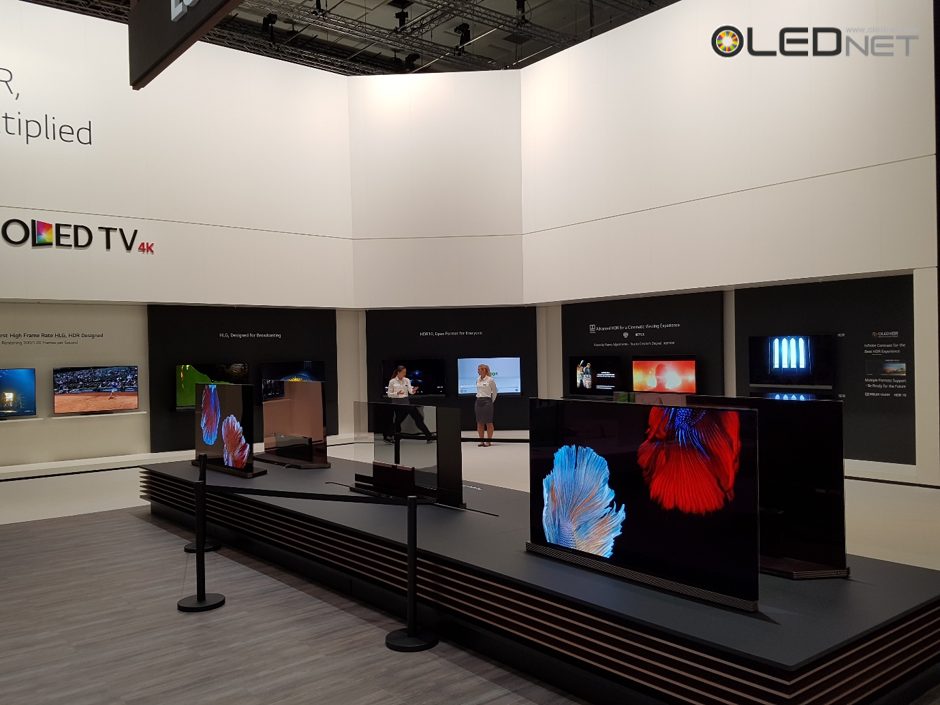
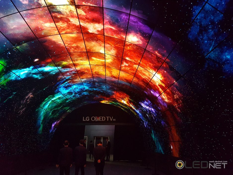
LG Electronics has displayed OLED TV on about half of the entire IFA2016 exhibition’s space, overwhelming the whole area.

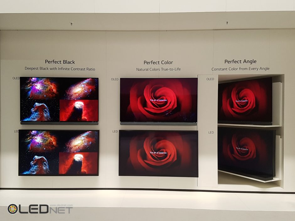
There is no need for words. You just have to enjoy the exhibition with your eyes.

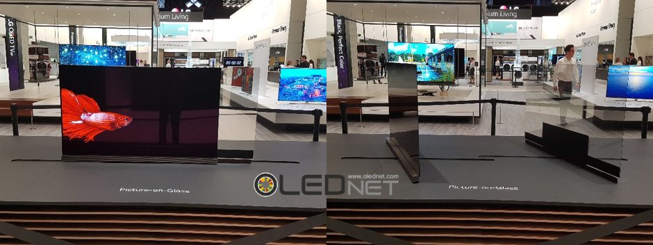
Apart from the image quality, LG promoted its slim product design by the expression “Picture on glass.”
There is no need for words. Exhibition is enough to show why OLED TV is better than LCD TV.

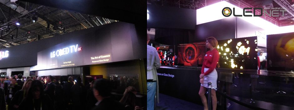
In the previous CES2016, LG Electronics booth was as dark as a movie theater. Presumably, it wanted to show the strength of OLED TV, “black”, well but it could rather be seen as a product that functions properly only in the dark.

CES2016 LG Electronics Booth: The light was as dark as a movie theater

However, the difference becomes definite when we compare the ceiling light of CES2016 and the light of IFA2016. It became brighter indeed. LG Electronics has changed.

It became confident enough to highlight merits of OLED TV even in a bright area. OLED panel structure of TV produced by LG Display has changed from bicolor structure laminated with three layers of B (blue) and YG (yellow-green) to a three-layers structure that uses B, R, and G to realize three colors. The efficiency and brightness of the colors have become overwhelmingly outstanding.

LG is not the son of darkness anymore. Through the exhibition, it expressed its confidence to have secured the quality to contend with LCD TV.

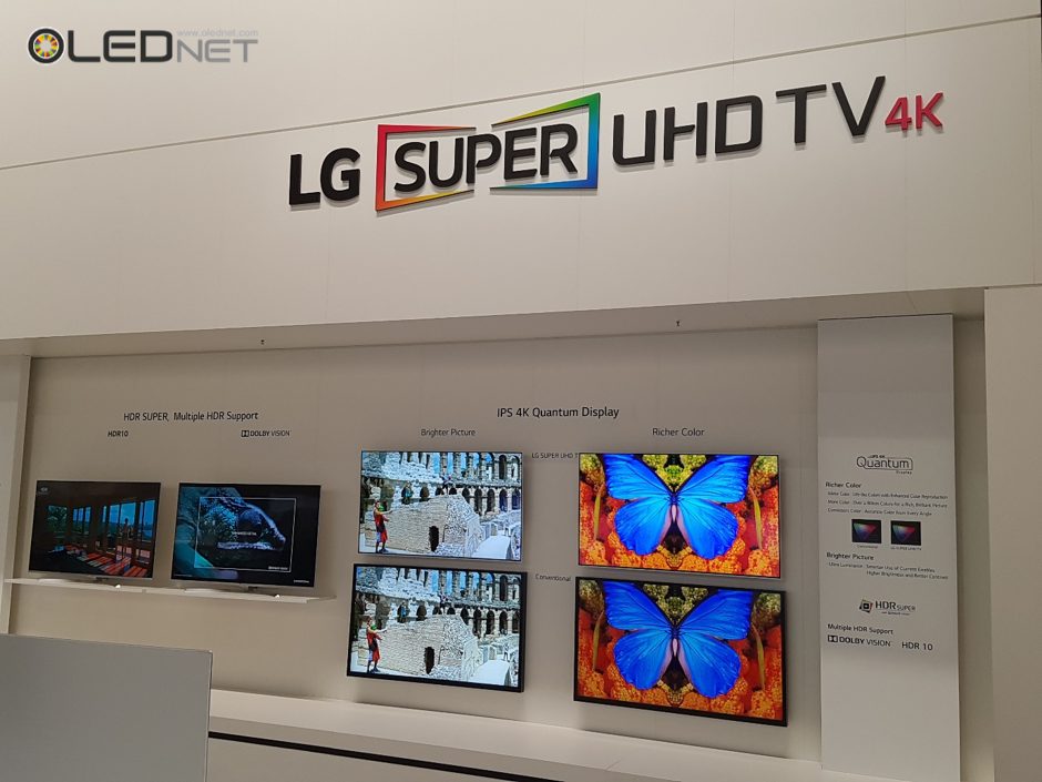
Of course, it also indicated to continue LCD TV business. It displayed LCD TV, which applied QD technology, in one side so that it’s not compared with numerous OLED TVs. The exhibition of LCD TV, positioned in the corner after losing power, shows that the time is getting closer for competitors to wake up from the illusion that LCD TV will last forever.