Posts

Sunic System’s Successful Demonstration of 1.1um Shadow Distance, High resolution up to 1500 ppi

Sunic System announced at 2016 IMID Business Forum that it succeeded in implementing 1.1um shadow distance by using plane source evaporation and 100um shadow mask. 1.1um shadow distance is able to manufacture 1000ppi~1500ppi high resolution.

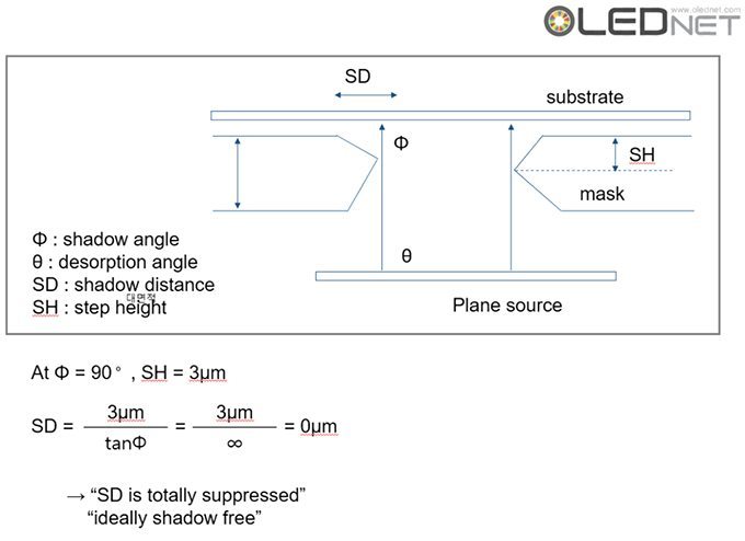
Plane source evaporation is a technology to evaporate OLED light-emitting material on metal plate, invert it, apply heat to the metal plate, and vertically evaporate OLED light-emitting material. When the shadow angle(Ф) of OLED light-emitting material evaporation is 90 degrees, the value of SD(Shadow distance, step height / tanФ) is zero (0) theoretically. So, it is possible to design thick and high resolution FMM, which means high-resolution AMOLED panel can be manufactured. This principle was announced for the first time at IMID 2016 Business Forum, attracting big attention.

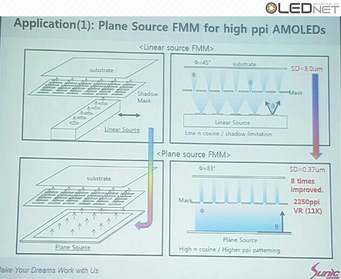
Sunic System Dr. Hwang Chang-hoon said “If we lower step height up to 3um by reducing the thickness of shadow mask based on this result, 0.37um shadow distance would be possible, which means we can manufacture maximum 2250ppi(11K) high resolution AMOLED panel. Accordingly, we will put spurs to development of 0.37 shadow distance”.

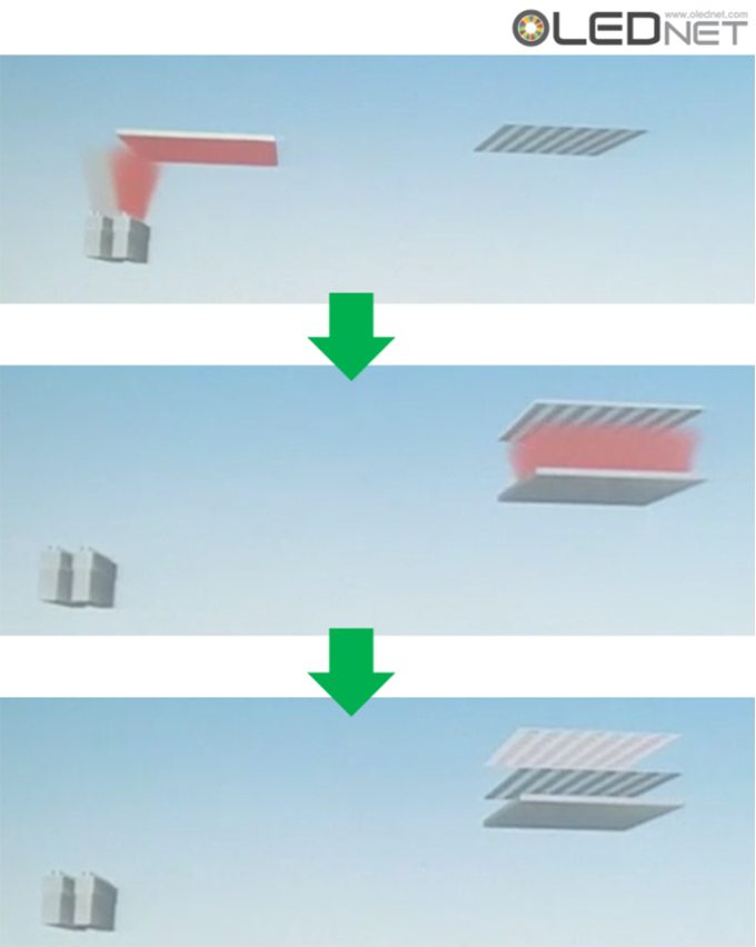
Also, he announced that co-evaporation of host and dopant that had been thought to be impossible in plane source has been resolved using flashing evaporation. He also proved that if donor film goes through flashing evaporation after co-evaporation of host and dopant, host and dopant can co-evaporate, and color control becomes easier by controlling dopant ratio to manufacture donor film.
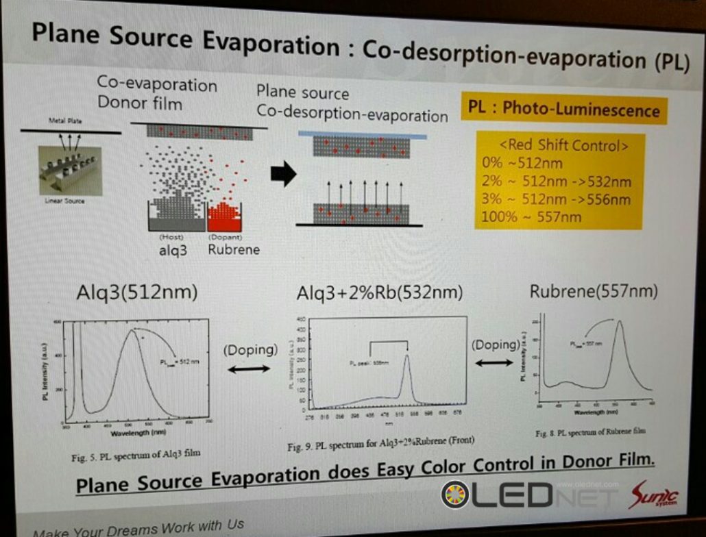
<Result of Color Control after applying Flashing Evaporation>
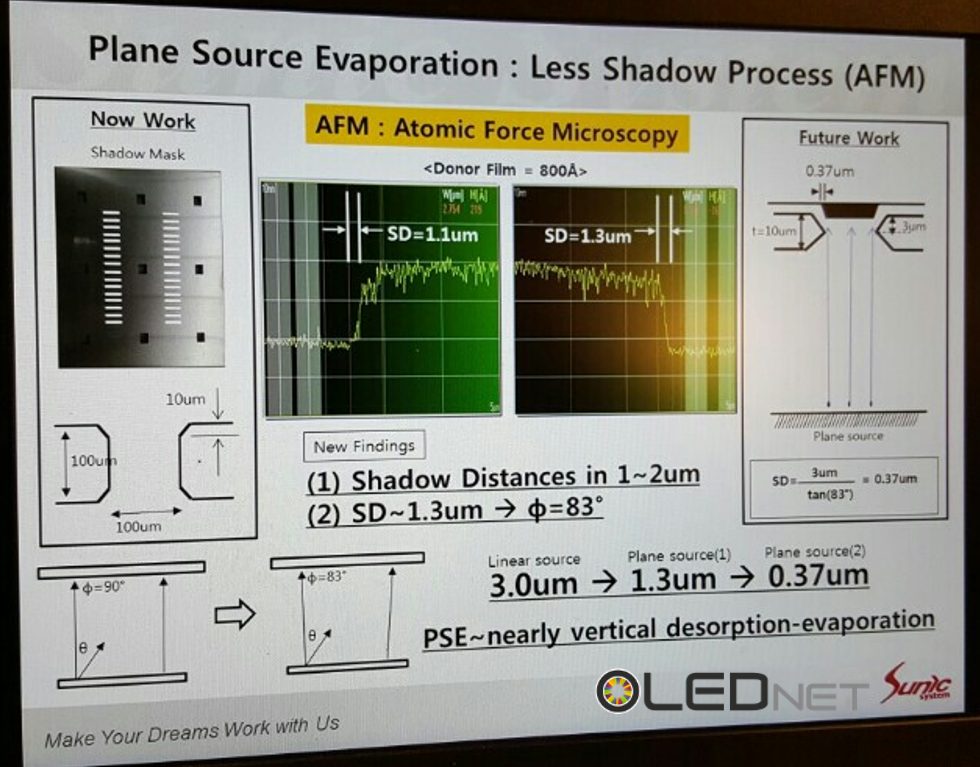
<Result of 1.1um Shadow Distance>

Sunic System Suggests High Resolution 11K AMOLED Panel Solution through Plane Source

Sunic System’s solution for 11K (2,250 ppi) AMOLED production revealed in IMID 2016 held in Jeju ICC, South Korea is receiving much attention.

In the 2nd OLED Korea Conference held earlier this year, Samsung Display’s principal engineer Insun Hwang told the attendees that high resolution is the key in VR, and approximately 2,000 ppi is required for suitable realism. He explained that the resolution of VR falls as the distance between the user and display is short and this is an issue that needs to be solved.

The highest resolution of the current AMOLED panel for mobile device is 806 ppi, revealed by Samsung Display in SID 2016. The technology being applied to AMOLED panel mass production is evaporating OLED emitting materials through heat from linear source, and depositing the OLED emitting materials onto substrate through fine metal mask (FMM).

However, during the deposition stage of the OLED emitting materials, due to the distance between the evaporation source and FMM, thickness of FMM, and distance between FMM and substrate, incidence angle (θ) is produced. Due to the incidence angle, shadow distance (SD) is generated. Because of the SD issues, mask thickness and step height that minimize SD have to be decided, and these are the main reasons for the FMM production difficulty.

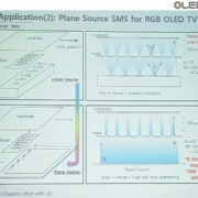
Plane Source Process, Sunic System IMID 2016

Plane Source Process, Sunic System IMID 2016

To solve these issues, Sunic System suggested plane source, instead of linear source, and reported that this will become a key technology for high resolution AMOLED panel. Plane source technology deposits OLED emitting materials on metal plate and vertically evaporates the materials through heat after reversing that metal plate. If OLED emitting material shadow angle (Ф) becomes 90, the SD (shadow distance, step height / tanФ) theoretically becomes 0. This means FMM can be designed to be thin and high resolution, allowing for high resolution AMOLED panel production.

Sunic System’s Dr. Chang Hun Hwang explained that plane source can reduce SD figure up to approximately 8 times compared to existing technology, and 11K (2250 ppi) AMOLED panel for VR use becomes possible. Through this 8K (200 ppi) RGB OLED TV panel production becomes possible in large area SMS evaporation technology.

Particularly, if plane source using SMS evaporation technology can be applied to large area, it is also expected to have significant impact on large area OLED panel production technology.

So far, inkjet printing technology applied solution process method has been mainly developed for RGB large area OLED panel production, but soluble OLED emitting materials’ performance fall short of existing evaporation OLED emitting materials. However, if plane source technology is successfully developed and applied, evaporation OLED emitting materials can be used. Accordingly, this could become large size OLED panel production technology that replaces solution process OLED.

Sunic System supplied Gen6 evaporator to LG Display, a first for a Korean manufacturing equipment company, and active mass production is expected to be possible from 2018.