[CES 2023] TCL CSOT 65″ 8K Inkjet Printing OLED
#Inkjetprinting #TCLCSOT #CES2023

https://oledkoreaconference.com

https://ubiresearch.com/en/

https://en.olednet.com/

marketing@ubiresearch.com
+82-2-577-4391
#Inkjetprinting #TCLCSOT #CES2023

https://oledkoreaconference.com

https://ubiresearch.com/en/

https://en.olednet.com/

marketing@ubiresearch.com
+82-2-577-4391
Samsung Display research center is accelerating the development of QNED as the next-generation display following OLED.
The reason Samsung Display is developing QNED as part of its large-size display business is that it is the only display that can produce the image quality that Samsung Display’s biggest customer, Samsung Electronics, can satisfy.
Samsung Electronics’ TV business direction, which has the world’s No. 1 TV market share, is to use QD to make color gamut better than OLED, and to use a display that can maximize HDR performance with high luminance and excellent gradation characteristics on a bright screen.
The only display that can satisfy the needs of Samsung Electronics is QNED.
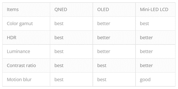
QNED is a self-luminous display and because it uses QD, it has the best color gamut, HDR, luminance, contrast ratio, and motion blur, etc., and is a product expected by Samsung Electronics.
It can be confirmed by the structure that QNED is the display with the best characteristics. QNED consists of a pixel layer with a nano-rod LED on the TFT structure of 3T1C used in large OLEDs, and a color conversion layer consisting of QD and CF (color filter) on top.
In OLED, electrodes (cathode and anode) and electrode line for transmitting a signal to a pixel are located above and below the light emitting material, whereas in QNED, both the signal transmitting electrode (pixel electrode) and electrode line are located on the same plane. In addition to the pixel electrode, the QNED additionally includes a reflective electrode to increase light output efficiency. The pixel electrode serves as an alignment electrode for aligning the nano-rod LED.
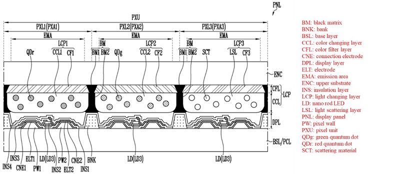
< QNED section structure >
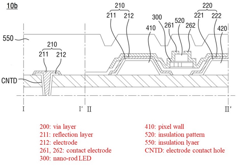
< QNED pixel structure >
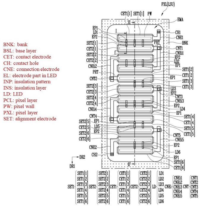
< QNED pixel planar structure >
Looking at the planar structure of a QNED pixel, a plurality of pixel electrodes are connected in series in one pixel, and a nano-rod LED is positioned between the pixel electrodes. The pixel electrode is on the pixel wall (PW) formed of an insulating material, and each pixel is surrounded by a bank (BNK) to separate regions.
The core technology of QNED is driving technology and sensing technology.
The driving technology includes a driving technique for aligning nano-rod LEDs and a driving technique for uniformly controlling pixels that may have a deviation in the number of nano-rod LEDs. The alignment circuit includes switching elements for each pixel, and the switching element applies an alignment signal to the pixel. The alignment state of the nano-rod LED is determined depending on which alignment signal is given to each pixel.
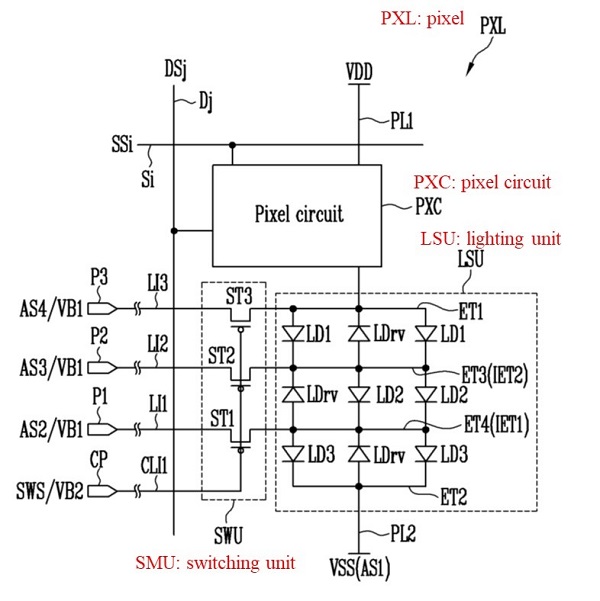
< Drive circuit for alignment >
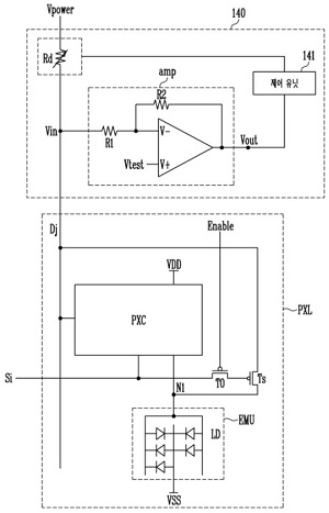
< Sensing transistor for checking alignment >
The most important driving technology is a technology that supplies current to each pixel so that the luminance can be uniform across the entire screen even if the number of nano-rod LEDs per pixel is different. It is a method of controlling each pixel based on the data read from the sensing transistor.
[QNED Technology Completion Analysis Report] details the sensing transistor, sensing wiring, and sensing signals that can check the nano-rod LED alignment status on the panel.
As sensing technology, there are sensing technology (sensing transistor) designed inside QNED and sensing technology used in QNED manufacturing. The sensing technology used to manufacture QNEDs is inherent in inkjet systems. There are three sensing technologies in the inkjet system: the number of nano-rod LEDs in the ink and the viscosity analysis of the solvent, the analysis of the number of nano-rod LEDs sprayed on the panel, and the analysis of the nano-rod LED alignment state.
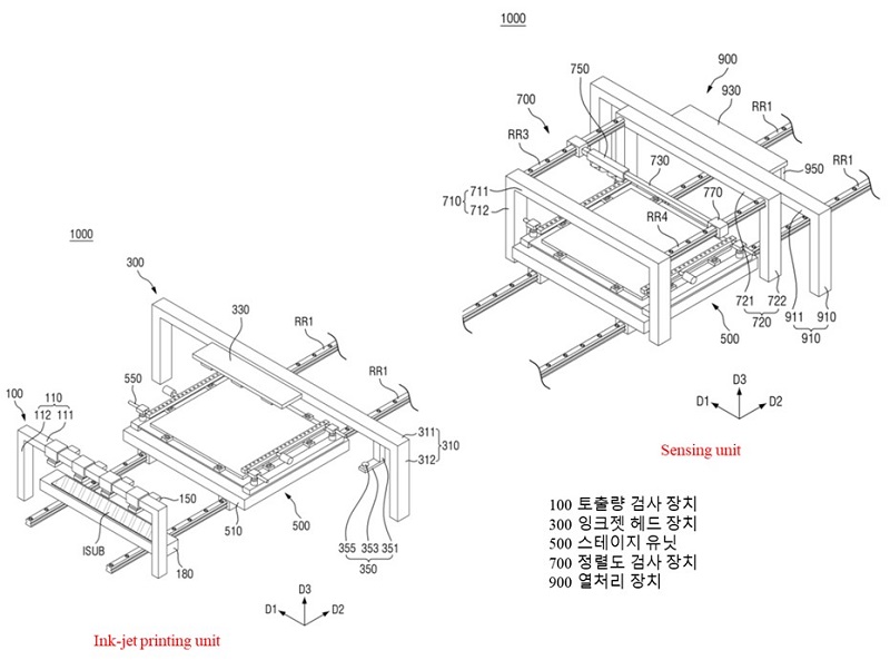
< Inkjet system configuration >
QNED has already proven that 4K 65 inches can be driven two years ago. Samsung Display is concentrating on finishing work to secure the screen uniformity of QNED.
At the 28th FINETECH JAPAN held in Tokyo, Japan from December 5 to 7, 2018, JDI and JOLED announced that they would intensify their cooperation in order to target the middle-sized OLED market.
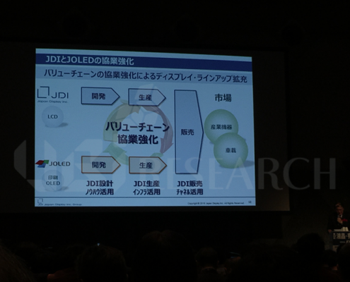
JDI announced that it will actively promote JOLED’s solution process OLED to medium-sized OLED markets such as industrial display markets or automotive display markets through its own design know-how, production infrastructure, and sales channels,.
In particular, JDI announced that it will provide new value to next-generation automotive fields along with JOLED such as support for safety such as electronic mirrors and displays for A/B pillars, new interface functions, movie appreciation using 4-8K displays, and the displays that are harmonized with interior design such as curved surfaces and big screens.
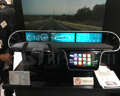
JDI and JOLED also shared booths for exhibition. JOLED introduced 21.6-inch FHD OLED monitors for e-sports and medical applications. In addition, it introduced a number of medium-sized OLEDs such as 12.3-inch HD OLED for automobiles, 12.2-inch FHD flexible OLED, 27-inch 4K OLED for home interior, and 21.6-inch 4K flexible OLED with cylindrical form. It also showcased large OLEDs such as 54.6 inch 4K OLED.
On the other hand, JOLED announced in July, 2018 that it would open its Nomi office for mass production of solution process OLED. Based on 5.5 generation glass substrates, Nomi has production capacity of 20,000 glass substrates per month and plans to mass-produce in 2020.
JOLED, the world’s first to successfully commercialize solution process OLED products, announced that it had raised a total of 47 billion yen as a third-party capital increase.
According to JOLED, Denso will invest 30 billion yen, Toyota Tsusho 10 billion yen, Sumitomo chemical 5 billion yen and SCREEN Finetech Solutions 2 billion yen. JOLED is known to cooperate with Denso to develop automotive displays and Sumitomo chemical to develop OLED materials for solution process.
In particular, Denso has been mainly using TFT-LCD for automotive displays, but it is expected to lead the development for applying lightweight and easy-to-shape OLED to automobile interior through this investment.
It is expected that this funding will accelerate the establishment of production system for the mass-production of JOLED’s solution process OLED. JOLED announced on July 1 that it would set up a “JOLED Nomi Office” in Nomi-city, Ishikawa, and aim to operate in 2020.
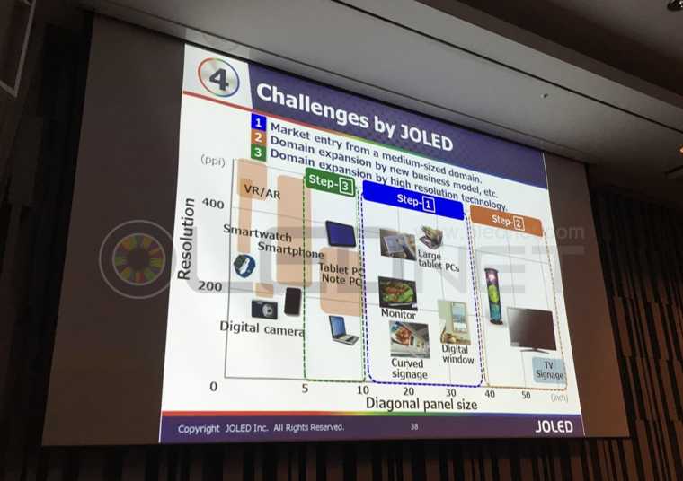
Major production products are medium-sized (10 to 32-inch) solution process OLEDs that will be used for cars or high-end monitors. Also, Toshiaki Arai, chief technologist of JOLED announced that they would target the middle-sized OLED market with solution process OLED, at the 2018 OLED Korea conference hosted by UBI Research in March.
UBI RESEARCH / CEO:Choong Hoon Yi / Business License Registration Number 220-87-44660
ADDRESS: A-1901, Samho Moolsan Bldg, 83, Nonhyeon-ro, Seocho-gu, Seoul, Republic of Korea (Zip) 06775 TEL:+82-2-577-4390 / E-MAIL:marketing@ubiresearch.com
