Posts

[IMID 2022] ETRI to Show ‘Stacked QD-OLED’ With Top Glass Removed

At IMID 2022 held in BEXCO, Busan, from August 23rd to the 26th, ETRI held an exhibition and presentation, ‘Development of QD-OLED Technology with Fine Quantum Dot Pixel Array using Inkjet Printing Process’.

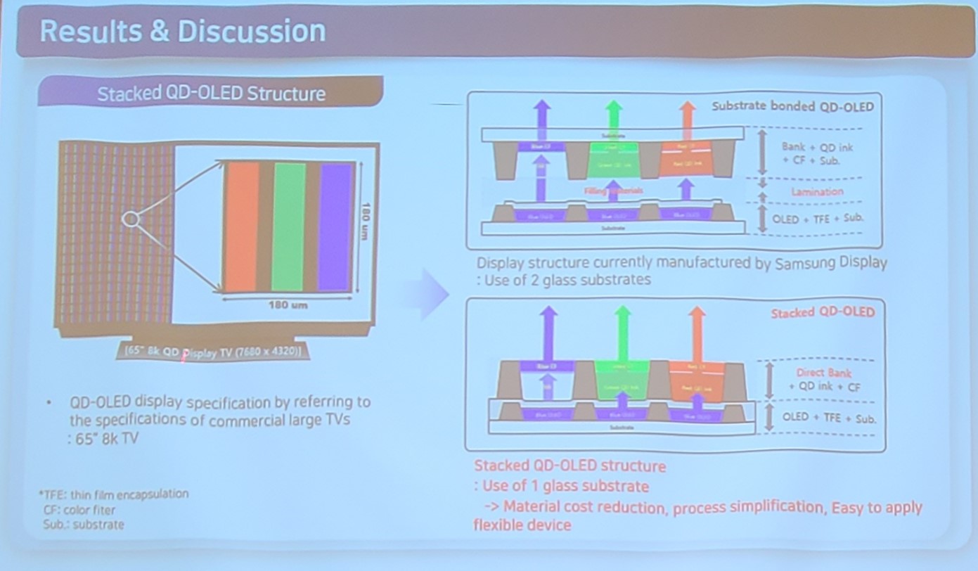
Stacked QD-OLED structure/ ETRI

Stacked QD-OLED structure/ ETRI

Two glass substrates are used in the QD-OLED produced by Samsung Display, but the ‘Stacked QD-OLED’ developed by ETRI has a structure in which the glass with the QD color conversion layer is removed. In the stacked OLED, TFE and BM are formed on the light emitting layer, and the QD color conversion layer is formed by the inkjet printing process instead of the lamination process. The ‘Stacked QD-OLED’ structure has advantages such as material cost reduction and process simplification compared to the existing method.

ETRI explained that there are advantages of material cost reduction and process simplification compared to the existing process through this, and the thickness of the QD color conversion layer can be made thicker than before, resulting in a higher color conversion rate and less blue light leakage.

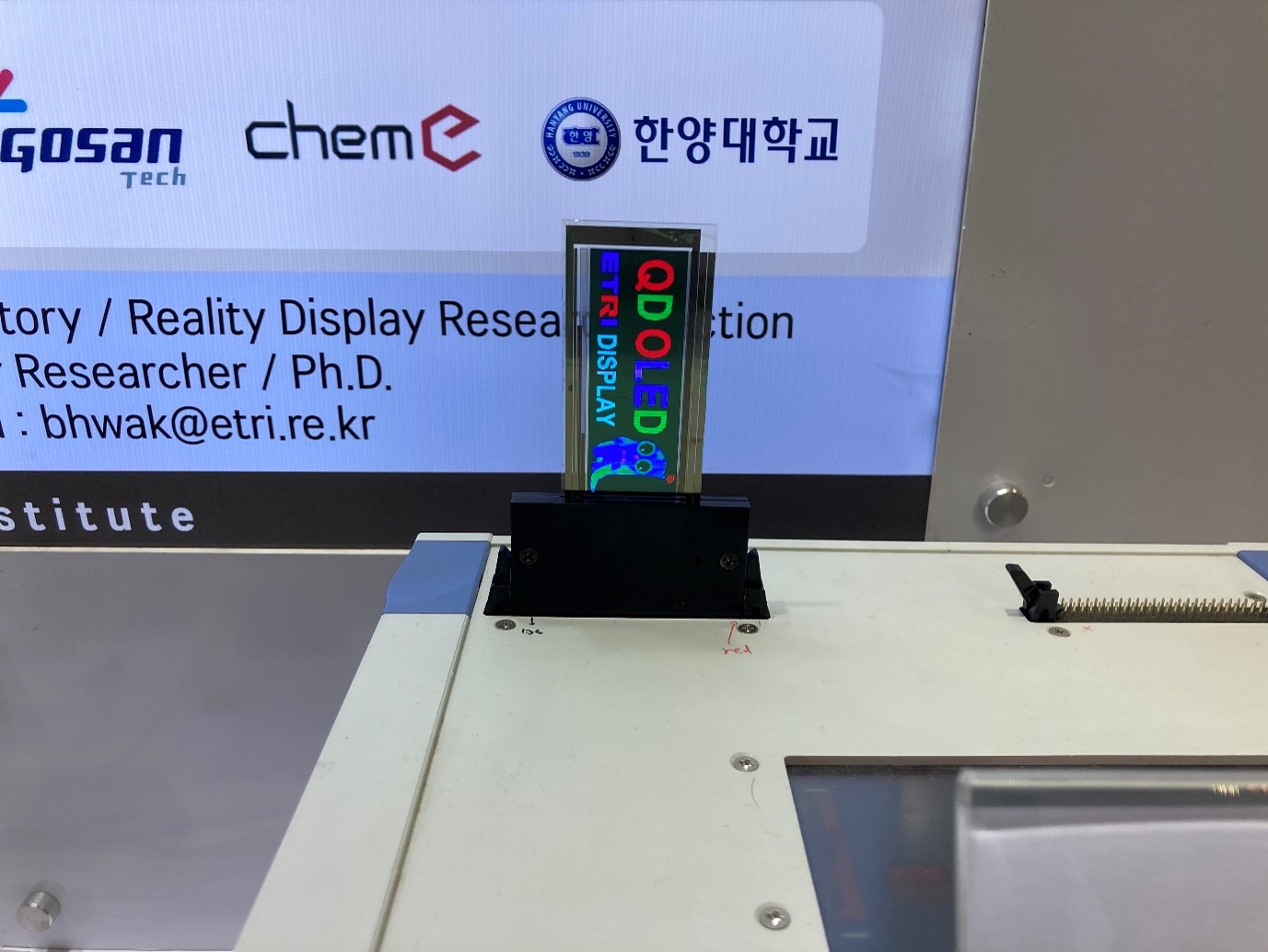
Meanwhile, ETRI collaborated with Kosan Tech for inkjet module head, Duksan Neolux for black bank material, and Chem e for QD material to develop ‘Stacked QD-OLED’.

‘Stacked QD-OLED’ Developed by ETRI

‘Stacked QD-OLED’ Developed by ETRI

▶ OLED Display Report Sample Download

ETRI’s Development of OLED Display With A Graphene Transparent Electrode

Reporter : Hana Oh(HanaOh@ubiresearch.com)

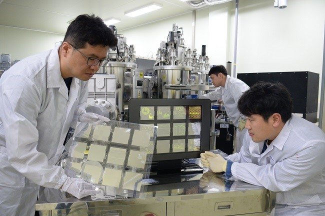
Researchers from Korea’s ETRI Institute developed a graphene transparent electrode for OLED display. Especially, they developed the process of patterning a graphene transparent electrode in exact size and shape on a large-sized substrate. Its application to smart watch requiring flexibility will be available.

ETRI(Electronics and Telecommunications Research Institute) has succeeded in developing a display with the electrode using graphene, a dream new-material, rather than using ITO(Indium Tin Oxide) that has been often used as existing electrodes for OLED display.

The successful display substrate is the current world’s largest one of 370mm x 470mm, a 19-inch monitor in size. The thickness of graphene electrodes is less than 5nm.

ETRI expects that if the graphene is deposited on flexible substrate, thin and flexible display will be feasible. Furthermore, it will become the source technology that can be used for manufacturing wearable devices applicable to clothing or skin.

In general, OLED is stacked with substrate, ITO transparent electrode, light-emitting organic layer, and anodized aluminum. The researches replaced typical ITO with grapheme.

In particular, ITO that has been used as existing electrode has a disadvantage of being made of fragile glass. Therefore, the display manufactured with this technology will clear up the problem of fragile transparent electrode.

ETRI developed graphene growth technology and oxide technology to be applied as an OLED transparent electrode by making a large-scale substrate in collaboration with Hanwha Techwin Co.,Ltd, and secured the grapheme transparent electrode fabricating and process technology with the sheet resistance of 60Ω/m² and the transmittance of 85% applicable to OLED. Especially, ETRI developed the world’s first micro-patterning process that is absolutely required for the display process.

Using this technology, ETRI successfully lighted the world’s largest grapheme electrode OLED panel of 370mm x 470mm. The finding of this study, which was published and demonstrated at 『Graphene 2017』, the world’s largest graphene conference held in Barcelona, Spain in early April, 2016, was highly acclaimed.

The researchers started to research grapheme transparent electrodes for OLED, based on the 4-year support of the Ministry of Trade, Industry and Energy(MOTIE) and Korea Evaluation Institute of Industrial Technology(KEIT) from 2012. They successfully developed a 100mm x 100mm OLED panel last year through the recent world’s largest demonstration, starting with a 7mm x 10mm coin-sized one, at the end of 2015, leading to the higher applicability of a grapheme-based display.

They said they will develop the display with a plastic substrate instead of a glass substrate. It is possible to manufacture a wearable OLED device if grapene is attached to plastic substrate, ETRI added.

ETRI’s Flexible Device Research Head Cho, Nam-sung said “The realization of a general expectation that grapheme would be applied to OLED display is very significant. We expect it will be successfully deployed on an commercial scale through large-scale grapheme film, OLED panel technology, and flexible OLED panel technology.”

This technology is expected to edge ahead from the later competitors including China as the core technology that can further increase the level of flexible OLED displays.

Transparent Electrode Needs Development for Next Generation Display to Surge

Recently, with various research results regarding transparent electrode, interest in next generation transparent electrode is increasing.


In early December, UNIST (Ulsan National Institute of Science and Technology) developed printing technology that can arrange the Ag nanowire in the direction chosen on top of substrate. Ag nanowire is transparent electrode that can be applied to large area flexible touch panel and display products. This technology allows the surface to be flat through the fusion of nanotechnology to the existing printing process and increases transmittance.


Around the same time, ETRI (Electronics and Telecommunications Research Institute) developed technology that replaces thin metal electrode on top of OLED substrate with graphene transparent electrode. The metal electrode that were being used in OLED was mostly silver (Ag) material, but due to the reflection of internal light, the viewing angle changed depending on the angle. The external light also affected picture quality due to reflection. The newly developed technology used graphene that mostly does not reflect internal/external light as transparent electrode and improved transmittance and picture quality.


At present, ITO (indium tin oxide) is most widely used as transparent electrode materials. However, the supply is limited and flexible electronic device application is narrow. As such, the demand for the development of new materials that can replace this is greatly increasing. Particularly, as ITO is not suitable for stretchable device, the next generation transparent electrode development is considered to be a key issue for future display.


At 2016 Production/Process Technology Development and Application Cases by Flexible Transparent Electrode and Film Materials Seminar (December 17) held in Seoul, South Korea, Dr. Won Mok Kim of KIST (Korea Institute of Science and Technology) discussed, of many flexible transparent electrodes, TCO (transparent conductive oxide) production and process technology through presentation titled ‘TCO based flexible transparent electrode production and process technology development trend and applications’.


Of the transparent conductive materials, oxides have been researched the longest, and they are most widely used transparent conductive materials. Oxide including conductive materials have optical band gap of ≥3.0 eV and therefore has high transmittance and can be flexible. Kim revealed that TCO needs further improvement in conductivity and transmittance for display application.


Regarding transparent body, when refractive indexes of components are different, the path of light through the transparent body is refracted. When this occurs, the object becomes hazy although transparent. Haze is quantified and used to assess the transparent body’s performance. Kim explained that for solar cell the haze is purposefully increased to transmit more light to the internal active materials. However, if the display is clouded the clarity of image is reduced and therefore haze has to be lowered. To achieve this, Kim reported that the TCO’s surface roughness has to be reduced.


Kim revealed that there are two issues, temperature and flexibility, when TCO is used as transparent electrode. ITO’s conductivity is highest at 300 ℃, and for ZnO it is around 200 ℃. Channel cracks could occur with TCO when higher than bending strain is applied, and the crack could snap when it is bent further, destroying the device performance. Kim explained that to increase the bending strain, the thickness has to be reduced. However, when doing so as the sheet tension increases, the process has to be designed carefully considering the tradeoff.


Transparent electrode could be applied to display, solar cell, touch panel, and lighting among others and therefore requires much development. Although oxides have been long researched as transparent electrode materials, Kim concluded that even more diverse value can be created through fusion with next generation materials.


그림1

OLED and Graphene Together Achieves Innovative Technology

By Choong Hoon Yi


Korean research team is expected to greatly improve display’s transmittance and picture quality through fusing graphene technology, focus of much attention as the new material to OLED technology.


On December 15, ETRI (Electronics and Telecommunications Research Institute) replaced the thin metal electrode that was used as transparent electrode on top of the OLED substrate with graphene transparent electrode, and succeeded in developing original technology that is conductive and transparent.


This research results were presented in Scientific Reports, a journal from the publishers of Nature on December 2.


The metal electrode used in OLED until now has been mostly silver material, but due to the reflection of internal light, the viewing angle changed depending on the angle. The external light also affected picture quality due to reflection.


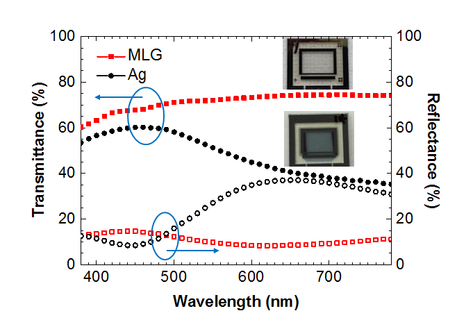
In order to solve this problem, ETRI research team focused on graphene that mostly does not reflect internal/external light. By replacing the material, the team reported that the transmittance increased by approximately 40% and reflectance improved by approximately 60%.


OLED was successfully lighted by attaching graphene transparent electrode to the organic layer on top of the film form (23 x 23 mm, 30 ㎛ thickness) of substrate. The research team believes this will be able to contribute much when applied to transparent OLED display and white OLED-based large area OLED display in future.


Particularly, unlike the existing vacuum process OLED production method, this technology can be employed via lamination where film is attached to the organic layer and graphene. Therefore, OLED can be produced through simpler process. It is expected that this can be evolved into production technology using roll to roll process.


Additionally, ETRI, together with Hanwha Techwin, is working on applying graphene transparent electrode to OLED’s lower electrode through collaboration of high quality graphene thin film electrode materials. The related technology development results were published online by The IEEE (Institute of Electrical and Electronics Engineers) of Selected Topics in Quantum Electronics.


ETRI’s Dr. Jeong-Ik Lee (soft I/O interface research section) anticipated that “this technology will be able to play a role in widening the gap with latecomer countries in OLED industry where challenging latecomers are strong”.


This research was carried out through Korea’s Ministry of Science, ICT and Future Planning and Institute for Information & Communications Technology Promotion (IITP)’s “Energy reducing environment adapting I/O platform technology development for future advertisement service” project and Ministry of Trade, Industry and Energy and Korea Evaluation Institute of Industrial Technology’s “Substrate size 5.5 generation or larger graphene film and OLED device/panel foundation and application technology development for graphene materials OLED transparent electrode and thin film encapsulation application”.


ETRI is planning to additionally develop sheet tension reducing technology by manufacturing metal in thin, grid forms and enlargement technology to produce mobile display size within 2016.


Through this technology, the research team produced 6 international patent applications and 6 papers. ETRI is intending to transfer the technology to graphene film and display panel companies among others. Commercialization is estimated to begin after 3 years.
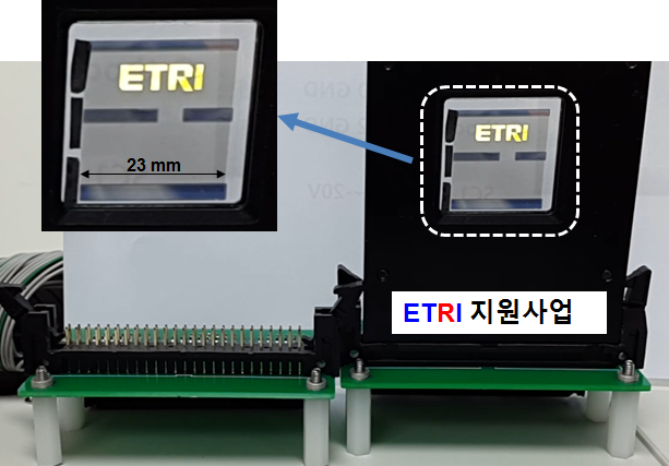
1.Graphene transparent electrode applied lit OLED
1. Graphene transparent electrode applied lit OLED


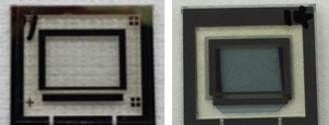
2. OLED with existing thin metal electrode and graphene electrode OLED comparison (Left: Graphene, Right: Thin Metal, Ag)
2. OLED with existing thin metal electrode and graphene electrode OLED comparison (Left: Graphene, Right: Thin Metal, Ag)


3.Film including graphene transparent electrode applied to lamination process using OLED production

3. Comparison graph of existing thin metal electrode OLED and graphene electrode OLED


4.Film including graphene transparent electrode applied to lamination process using OLED production

4. Film including graphene transparent electrode applied to lamination process using OLED production
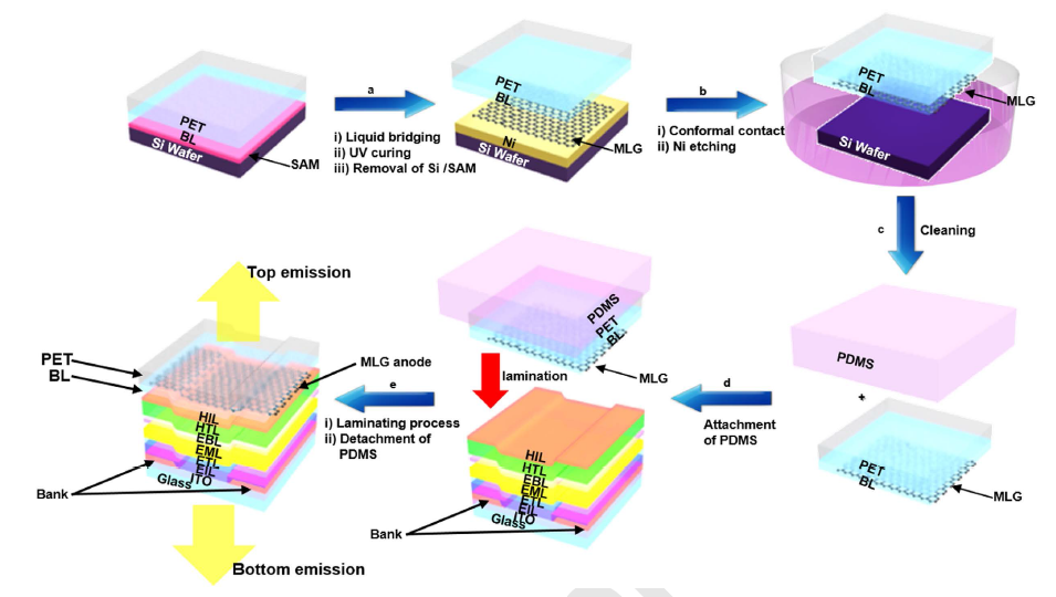
 

5.Graphene transparent electrode OLED Production Process

5. Graphene transparent electrode OLED Production Process


[Process Explanation]

After manufacturing laminated film, formed with bonding layer (BL) and PET film, using surface treated substrate, graphene transparent electrode is transferred on to the bonding layer. By laminating the laminated film that includes graphene transparent electrode on the substrate (lower electrode and organic layer), OLED where graphene transparent electrode is used as upper electrode is complete.
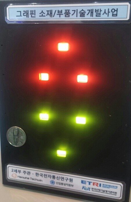
 

6.Graphene OLED of diverse colors

6. Graphene OLED of diverse colors
ETRI Reveals Graphene Applied OLED Lighting

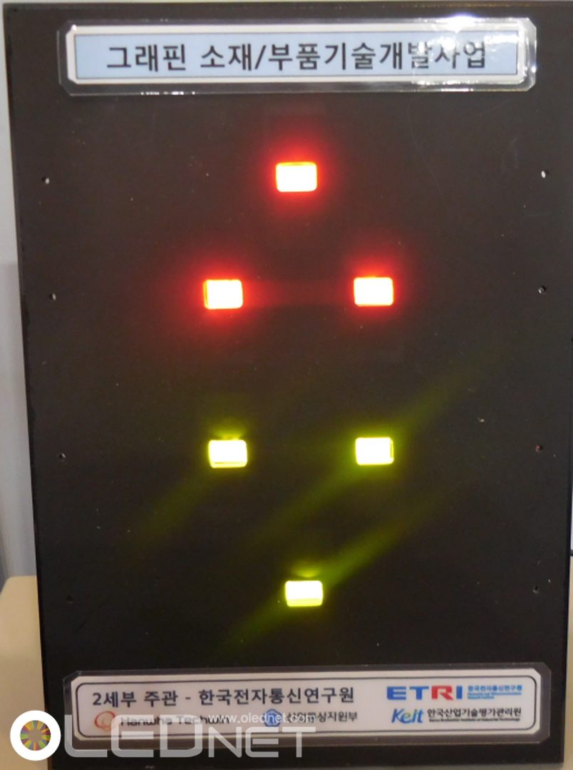
At R&D Korea 2015 (November 19-21), ETRI (Electronics and Telecommunications Research Institute) revealed OLED lighting and graphene related research results.


Since 2013, ETRI has been participating in ‘Graphene Applied OLED Device/Panel Technology Development’ project as a supervising organization. This project is a part of ‘Graphene Device/Component Commercialization Technology Business’, which is a Korean national project. This project’s ultimate aims include development of graphene electrode material with ≥15Ω sheet resistance, ≥90% transmittance, 3nm thickness, ≤5% sheet resistance uniformity, ≤5nm surface profile, and ≥5.5 generation area, graphene based protection layer that can be used for 5.5 generation 55inch OLED panel with ≤10-6 g/m2 WVTR, graphene anode OLED with ≥90% external quantum efficiency compared to ITO anode OLED, and diagonally 1300mm OLED panel prototype.


ETR1


In this exhibition, ETRI presented OLED lighting that used graphene as the electrode. ETRI’s Dr. Jeong-Ik Lee explained that recently interest in graphene electrode is increasing to replace ITO electrode and to apply graphene electrode, optical, electrical, and process issues have to be considered. When graphene is used as OLED electrode instead of ITO, thickness and refractive index change optically and electrically energy levels change, and these have to be considered when designing. He also emphasized that in terms of process, it has to be designed keeping in mind of before and after process of electrode procedure. Dr. Lee revealed that at present optical and electrical issues are solved while the process issues are in research stage, and they are planning to present the results of this research within this year.


Graphene, with its high resistivity, is known as next generation electrode material favorable to flexible and foldable. Dr. Lee pointed out that graphene has wider viewing angle than ITO when used as transparent electrode is another important advantage, and particularly as white light source’s spectrum cannot change according to the viewing angle, graphene is suitable for application.


Graphene is a key material with a wide arrange of applications, it is being developed in diverse areas such as OLED encapsulation as well as in electrode sector. The Ministry of Science, ICT and Future Planning of Korea estimated that domestic graphene market will record 19 billion KRW until 2025. Korea Evaluation Institute of Industrial Technology, the organization in charge of this national project, gave their target as developing 9 top technology through graphene and achieve 17 billion KRW sales. Regarding this, Dr. Lee emphasized compared to other countries, Korean investment in graphene is relatively low and that now is the time for the Korean corporations and government agencies to pay more attention higher value-added businesses.

[Automotive Display Seminar] Automotive Display, Urgent Transparent Display Technology Development Needed

By Choong Hoon Yi


On November 13, Automotive Display Development Technology and Commercialization Planning seminar was hosted by Educational Center of Future Technology in Yeouido, South Korea.


KATECH (Korea Automotive Technology Institute)’s Dr. Sun-Hong Park explained that “as the automotive display market grows, display market’s domain is expanding” and announced “market for CID (Central Information Display) that mainly functions as navigation device and HUD (Head Up Display) that can show mileage and speed is steadily growing since 2008 and it is anticipated to grow considerably in future”. He added that particularly, 7inch or larger CID is increasing its market share in display market and that CID is becoming larger. He also mentioned that with the increase of traffic accidents from driver’s lack of attention to the road, HUD that can show information on the front window is necessary. However, legibility issues due to brightness and reflectiveness and technological issues such as integration with other display device need to be solved.


Dr. Sun-Hong Park of KATECH (Korea Automotive Technology Institute)

Dr. Sun-Hong Park of KATECH (Korea Automotive Technology Institute)


Dr. Chi-Sun Hwang of ETRI (Electronics and Telecommunications Research Institute) compared display technology that can actualize transparent display, and technological issues to be solved in order for it to be applied to automotive. Hwang explained that although display technology that can produce transparent display include LCD, OLED TFEL (thin film EL), HUD (projection) among others, AMOLED is the most suitable considering resolution and transmittance. Although LCD technology level is at commercialization stage, as the transmittance is not high it can interfere with the driver’s viewing field. He also added that “poly Si TFT technology performance is good, transmittance is limited. However, oxide TFT technology’s transmittance is high and performance is continuing to improve, it needs to be more actively developed”. To be used as an automotive display, it has to meet certain conditions such as temperature, production cost, and brightness to be an automotive component as well as being placed in the suitable location in the driver’s viewing field; compared to other general display, automotive display is facing higher number of technical issues.


Dr. Chi-Sun Hwang of ETRI (Electronics and Telecommunications Research Institute)

Dr. Chi-Sun Hwang of ETRI (Electronics and Telecommunications Research Institute)


Source: Dr. Chi-Sun Hwang of ETRI (Electronics and Telecommunications Research Institute)

Source: Dr. Chi-Sun Hwang of ETRI (Electronics and Telecommunications Research Institute)


With the focus on the transparent display from automotive display industry, the interest in the technology needed for the application to automotive is also increasing. In order to lead the automotive display market, understanding of automotive components’ characteristics and effort to solve the diverse issues facing the optimized driving condition are required as well as knowledge of display itself.

[IWFPE 2015] What Will Replace ITO?

2015 IWFPE (International Workshop on Flexible & Printable Electronics) was held at Le Win Hotel in Jeonju, South Korea (November 4-6). During the workshop, many OLED display related presentations commented on ITO’s replacement material.


Dr. Jennifer Colegrove, CEO of US research company Touch Display Research, discussed hot trends of 2015-2016. Dr. Colegrove included high resolution, transparent display, wearable device, and flexible display in the hot trends. Of these she pointed out ITO replacement material regarding touch panel. She mentioning metal mesh, silver nanowire, CNT, and graphene as materials that could replace ITO. Dr. Colegrove added that the material has to be flexible in order to be applicable to flexible display and needs to have high efficiency.


그래핀


Hanwha Techwin’s Dr. Seungmin Cho announced that graphene, which has higher uniformity compared to ITO, will be the material of future. With lower resistance than ITO, graphene shows good characteristics, but Dr. Cho explained that high cost and particles produced are issues that need to be solved. He also commented that China selected graphene related national projects and is striving to develop the technology.


Dr. Hyunkoo Lee of ETRI (Electronics and Telecommunications Research Institute) presented that the multi-layered graphene that ETRI, Sungkyunkwan University, and KAIST (Korea Advanced Institute of Science and Technology) co-developed will become the material that can replace ITO. He also introduced the results that as the transmittance is particularly high, it is suitable for transparent display, and compared to silver nanowire material in high resolution top emission structure, the display’s brightness is higher.


ITO replacement development is an issue for the future of display industry’s progress. It is estimated that research development on graphene as one of the ITO replacement electrodes will be actively carried out.


그래핀2

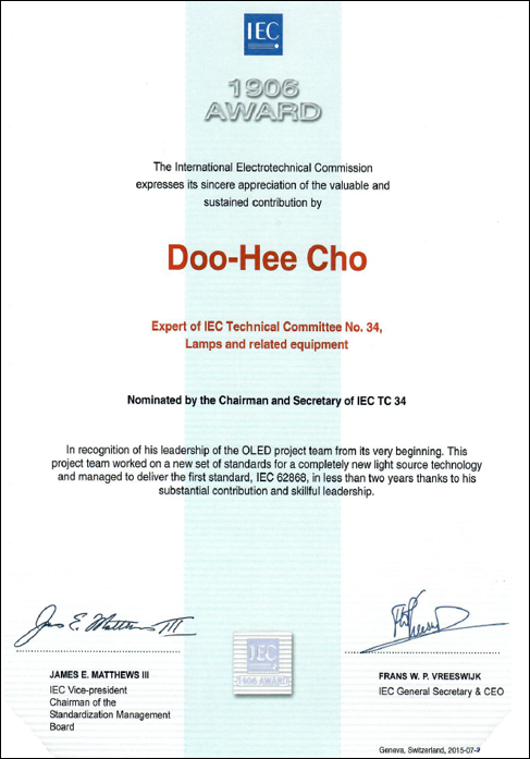
ETRI’s Doo-Hee Cho Receives IEC 1906 Award

On October 23, ETRI (Electronics and Telecommunications Research Institute) Information & Communications Core Technology Research Laboratory’s Dr. Doo-Hee Cho received IEC 1906 Award at World Standards Day ceremony. The IEC 1906 Award recognizes exceptional current achievements and it is presented by the International Electrotechnical Commission, one of the top 3 international standards organizations.


Dr. Cho has been active in IEC since his involvement in 2009. The activities include serving as the president of IEC·TC34 (lighting)’s OLED working group and establishment of IEC 62866: Organic Light Emitting Diode (OLED) panels for general lighting – Safety requirements.


Founded in 1906, IEC is one of the top 3 international standards organizations along with ISO (International Organization for Standardization) and ITU (International Telecommunication Union) with 83 member countries. IEC established IEC 1906 Award in 2004. Since then they have been selecting industry’s experts with outstanding contribution to electrotechnical standardization and IEC development and presenting the award annually. With this award for Dr. Cho, acceleration to OLED lighting’s international standardization and OLED lighting business growth are anticipated.


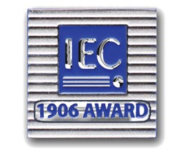
IEC 1906 Award Badge

IEC 1906 Award Certificate

Dr. Doo-Hee Cho