
[IMID 2015] UDC Develops OLED Patterning Technology with Less Masks
At present, FMM (Fine Metal Mask) is considered the main method for large area RGB OLED panel production. However, due to shadow effect, mask total pitch fluctuations, and mask slit tolerance issues, there is a yield limitation to this technology. This limitation increases as the resolution becomes higher; minimizing the number of FMM during the OLED panel production has been a key issue in RGB OLED production.
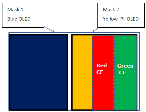
In SID 2014, through a paper titled “Novel Two Mask AMOLED Display Architecture”, UDC revealed a technology that can reduce the number of masks used in RGB-FMM method to 2 from previous 3.
Source : UDC, SID 2014
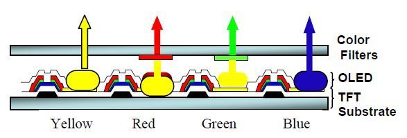
As shown above, this technology coats yellow and blue subpixels using 1 mask each. Following this process, green and red color filters are applied above the subpixels. Pixels are formed as illustrated below.
Source : UDC, SID 2014
UDC explained that this technology improves lifetime of the display overall and reduces energy consumption as blue voltage can be lowered. Additionally, tact time can be reduced through this technology, and increase the yield.
In IMID 2015, UDC presented research of the same title. However, the content of the presentation unveiled more developed research compared to 2014. First of all, in 2014, UDC announced that the panel’s lifetime could be improved by 2 times compared to the RGB method. In IMID 2015, UDC’s announcement changed the figure to 3.3 times increased lifetime.
UDC also revealed that the technology can be actualized through printing method, and has the advantage of being able to print 2 rows of pixels at once. UDC announced that this is most suitable when OVJP (Organic Vapor Jet Printing) applies the printing method.
A new technology called SPR (Sub-Pixel Rendering) was also announced by UDC in this paper. The 2014 SID paper included a method that did not uses SPR. As shown below in figure 1, 4 subpixels of RGY and B are used per pixel.
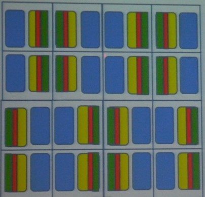
[Fig. 1], Source: UDC, IMID 2015
During IMID 2015, UDC presented APR technology applied pixel structure. Figure 2 shows 3 subpixels per pixel.
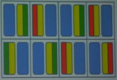
[Fig. 2], Source: UDC, IMID 2015
In this case, as the pixels can be arranged as shown in figure 3, smaller number of subpixels can be used.
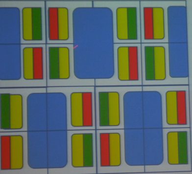
[Fig. 3], Source: UDC, IMID 2015
UDC announced that because APR technology allows the number of subpixels per pixel to be reduced to 3 or less, the number of data lines and TFT per pixel can also be reduced together.
UDC explained that this technology can be applied regardless of the display area or resolution, and will be able to be applied to different types of panels.
Leave a Reply
Want to join the discussion?Feel free to contribute!