Posts

[IMID 2017] Opening solution for next generation high-resolution OLED implementation

Various solutions for high resolution OLED implementation were released at iMiD 2017 held in COEX from October 18th to 19th. As the resolution of small and mid-sized OLEDs, which are currently being commercialized, is staying at the QHD level, the solutions released at this time have attracted a great deal of attention from display members.

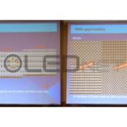
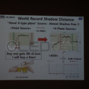
First, Hwang Chang-hoon, CEO of OLEDON, who is developing plane source FMM deposition technology, announced at the business forum, “The plane source FMM deposition technology currently being developed is the only alternative for ultra-high resolution OLED manufacturing at 2,250 ppi”. Hwang Chang-hoon CEO said, “We measured the shadow distance using a-step, and it was 0.38 μm. We can fabricate OLED device with 2,250 ppi only if we have this shadow distance.” “We are currently looking for shadow-free process conditions”

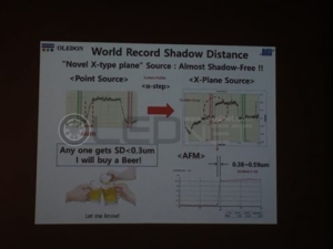
<Difference in shadow distance between point source and plane source>

In addition, Hwang Chang-hoon said, “We first co-deposited the host material and the dopant material on the metal plate to evaporate the deposited green donor thin film and measure the green target thin film with the same PL wavelength for the first time” and “Color control of target thin films made with plate sources can be controlled by the amount of dopant molecules in the donor film, so color control is expected to be easy”.

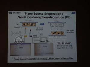
<OLEDON plane evaporation co-deposition material>

AP Systems, which recently announced the successful development of 1,000 ppi FMM using ultra-short pulse laser (USPL), exhibited 5.28 inch FMM of 825 ppi and 4.72 inch FMM of 677 ppi at this exhibition. A company official said, “By developing a burr-free laser process to solve the burr problem caused by the heat generated during the fabrication process, it is possible to fabricate not only FMM of 1170 ppi but also FMM of various shapes”.

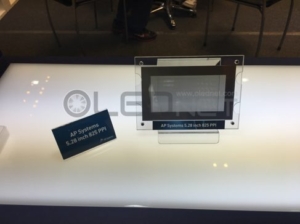
<5.28 inch 825ppi FMM of AP Systems>

Finally, Philoptics unveiled FMMs fabricated using electro forming, especially, FMM of 1,200 ppi, which attracted attention this time, was displayed separately in the VIP room. A company official said “We have secured the stability of the process for the production of 1,200 ppi FMM,” and mentioned “We plan to deliver it to panel makers for testing in the first half of next year, and aim to develop FMM at 2,000 ppi later.”

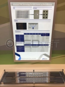
<FMM of Philoptics manufactured by electro forming method>

As such, in this iMiD 2017, various solutions for high-resolution patterning of OLEDs has been released. Recently, as the number of contents requiring high-resolution OLED such as virtual reality contents increases, interest of smartphone users are increasingly interested. It is worth noting which solution will enable the small to medium-sized UHD OLED era.

[iMiD 2017] JOLED announces printing-type OLED development trend and future road map

At the ‘IMID 2017 Business Forum’ held in COEX, Seoul from 18th to 19th, Toshiaki Arai, chief technologist of JOLED announced JOLED’s printing technology and future road map.

<JOLED’s Toshiaki Arai chief technologist>

Toshiaki Arai, chief technologist stated that a stable jetting technology at 220 ppi level has been currently secured; high resolution OLED with more than 300 ppi has been developed at Gen 8.5 but there are some issues such as jetting accuracy and stability.

Toshiaki Arai introduced TG-TAOS (top gate-transparent amorphous oxide semiconductors) TFT, which will contribute to saving the unit cost of OLED with excellent performance at low price.

He also announced the future strategy of JOLED, stressing that, instead of small and large OLED dominated by South Korean companies, the middle-sized OLED for tablet and monitor with more than 200 ppi. Joled is the only OLED panel maker that unveiled its 21.6 inch 4K RGB OLED in 2017, using printing process, and has pilot launched.

<JOLED’s 21.6 inch 4K OLED in application of printing method>

On the other hand, according to the Nihon Keizai newspaper in Japan, JOLED is reported to have invested 100 billion yen in mass production of printing-type OLED. In addition, Toshiaki Arai stated that the OLED test samples manufactured by printing process have been provided since this April and the mass production will realize in the second half of 2018.


[iMiD 2017] Samsung Display, Huge release of application using OLED

Samsung Display has received great attention by releasing a large number of applications using OLED such as VR and light field display in iMiD 2017 held in BEXCO, Busan from 28th to 31st August.

<Samsung Display booth>

First, Samsung Display comparatively exhibited a 3.5-inch OLED with 460ppi resolution for virtual reality and an 806ppi 3.2-inch OLED. A company official said “The higher the ppi, the better the experience of realism and immersion,” and mentioned “We are currently developing higher resolution OLEDs.”

<Comparison of 3.5 inch 460 ppi OLED and 3.2 inch 806 ppi>

In addition, Samsung Display exhibited OLED light field displays in the future display zone, and in the AMOLED zone, visitors can directly compare LCD and OLED.

A company official explained that “light field display is a technology that implements 3D by applying an optical lens on a panel, which is a little different from hologram using light interference effect.” And he said “We are developing a viewing angle that is wider than 30 °,” revealed “We now have pixel and lens alignment issues and optical design issues.”

<OLED light field display description and specification>

In the AMOLED zone, panels were displayed to directly compare the contrast ratio of LCD and OLED. The contrast ratio and color expressiveness of the OLEDs were clearly different from those of the LCDs, and a company official said, “These differences are the reasons why OLEDs are used in the Galaxy series.”

<Comparison of OLED (Left) and LCD (right) image quality>

Samsung Display has also introduced 1.3 inch circle OLED and 12 inch FHD OLED, which led to the great interest of the visitors during the exhibition.

[iMiD 2017] LG Display, Spur Development of 77 inch transparent flexible OLED

LG Display’s Kwon Se-Yeol senior researcher introduced the 77-inch transparent flexible OLED which had been introduced in June at IMID 2017 held in BEXCO, Busan on Aug. 30, and announced the applied technologies to realize this.

Kwon Se-Yeol senior researcher mentioned, “OLED is self-luminous, so it can be manufactured with a thin thickness because it does not need a back light unit. The thinner the thickness, the more flexible the OLED can be so that it is easy to implement flexible displays with OLEDs.” and forecasted. “It can be used in various fields such as signage and smart desk.”

The 77-inch transparent flexible OLED which is released this time is a top emission type for improved luminance. The transparent thin film encapsulation layer is applied, different from the conventional OLED TV or large flexible OLED, and two polyimide substrates are used.

Kwon Se-Yeol senior researcher said “We applied a transparent thin-film encapsulation layer instead of the existing metal encapsulation layer for the top emission method ” and explained “A white OLED light emitting layer and a color filter layer were formed on two polyimide substrates and cemented together. A barrier film and a multi-barrier were applied to the top and bottom of the polyimide substrates to prevent moisture and oxygen penetration.”

The Kwon Se-Yeol senior researcher then states that “flexural rigidity of the panel is mainly affected by the thickness of the polarizer and the encapsulant layer, so it is necessary to reduce the thickness in order to improve the flexibility”, and emphasized “By reducing the thickness of the encapsulant layer from 100 μm to 20 μm, we can reduce the strain on the OLED module from 0.36% to 0.21%, along with improved flexibility”.

In addition, he mentioned that surface reflection due to polyimide birefringence phenomenon, laser wavelength selection according to polyimide properties in LLO (laser lift off) process, and use of flexible OLED module are all covered, and technical development is continuing.

Meanwhile, LG Display has developed the world’s first 77-inch transparent flexible OLED with UHD (3840 × 2160) resolution, transmittance of 40%, and radius of curvature of 80R as part of the national project.

[iMiD 2017] AP Systems, Find FMM answers through USPL

At iMiD 2017 in BEXCO, Busan on 28th, AP Systems announced that it succeeded in developing 1000ppi FMM with USPL (ultra-short pulse laser).

Since FMM plays a role of depositing pixels and RGB organic materials, FMM serves as a factor that determines resolution and yield of OLED. At present, FMM is mainly manufactured by etching method. This method has a problem that a shadow phenomenon due to the precision, thickness, and weight of the fine pattern occurs, in order to solve this problem, various FMM manufacturing processes such as laser processing and electro-forming have been developed.

Among these, laser processing method has an issue of forming burrs around pin-holes due to the thermal effect caused by laser irradiation. These burrs increase the shadow interval of the FMM, which causes overlapping of patterns during RGB organic deposition, thereby degrading the resolution of the OLED.

AP Systems has developed a burr-free laser process that does not have burr phenomenon and further controls the taper angle.

The Burr-free laser process is a short-time irradiation of unidirectional pulses at a constant number of times, since the laser is not continuously irradiated, it minimizes accumulated heat energy and prevents burr formation. In addition, by controlling energy of the laser, it accumulates energy and forms taper.

In this way, AP Systems explained ‘they produced FMM with various shapes of fine pin-holes such as square, diamond, and polygonal shapes, as well as 1170ppi FMM’, and ‘’We also developed large-area FMM manufacturing equipment with USPL method’.

AP Systems also added ‘multi-beam and USPL is equipped for FMM manufacturing equipment so that it can improve productivity and realize UHD’.

Since the launch of the Galaxy Note4 in 2014, the OLED resolution has remained at the QHD level yet. In order to manufacture an OLED having a high resolution (UHD level or higher), it is necessary to solve various technical problems faced by FMM. Accordingly, it is noteworthy how USPL technology of AP Systems will affect the future OLED market.

<1000ppi FMM produced by AP Systems>

<various type of FMM produced by AP Systems>