GrapheneLab surpasses the ppi limit with a plated metal mask
GrapheneLab, a graphene commercialization technology company, announced that it is possible to manufacture FMMs over 800ppi using graphene.
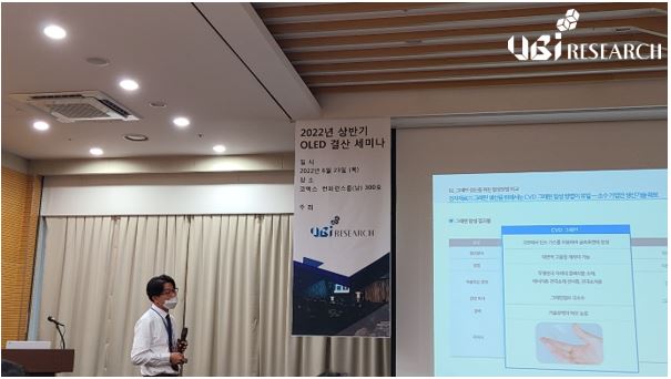
At the ‘UBI Research First Half 2022 OLED Settlement Seminar’ held at COEX in Samseong-dong, Seoul on the 23rd, GrapheneLab CEO Yong-duk Kwon said, “In the early 2000s, FMM technology, which started in the early 2000s, was not interested in the plating method. It is changing,”, and “After 2013, many patents related to the plating method FMM manufacturing technology have been applied, and it is easier to apply the plating method than the currently used etching method in order to go to high resolution.”
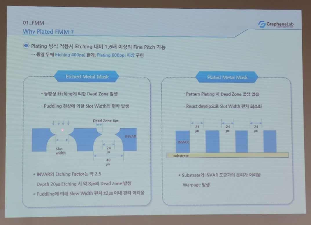
Next, CEO Kwon said, “We moved away from the existing limiting etching method FMM and applied the plating method FMM. Compared to the etching method, where 400ppi was the limit at the same thickness, the plating method realized more than 600ppi.”, “Etched metal mask has a dead zone of 8um in length due to the INVAR structure that becomes sharp like a dot when etching at a depth of 20um, whereas there is no dead zone during pattern plating of the plated metal mask.”
Lastly, CEO Kwon said, “For the MSAP electroforming technology, a low coefficient of thermal expansion with a thin thickness is required. As a result of measuring the coefficient of thermal expansion using TMA on the plated sample, it was measured up to 3.1ppm, and it went down to 2.5ppm without heat treatment.”