Jusung Engineering, 8th Generation Ultra-Thin OLED Encapsulation Equipment Technology Development to Preoccupy the Market and Achieve Localization [2022 Display General Workshop]
Jusung Engineering, 8th Generation Ultra-Thin OLED Encapsulation Equipment Technology (2022 Display General Workshop)

Jusung Engineering, 8th Generation Ultra-Thin OLED Encapsulation Equipment Technology (2022 Display General Workshop)

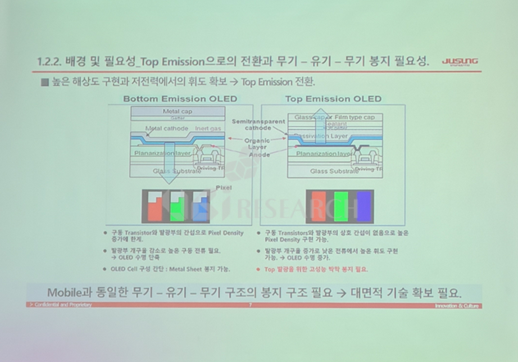
At the “2022 Display General Workshop” held at Pyeongchang Phoenix Park from November 9 to 11, 2022, H&iruja presented a research project on the development of an ultra-low damage cluster sputter system for mass-production of small and medium-sized OLEDs for 8.5th generation substrates.

H&iruja said, “It is important to improve yield and increase productivity using large substrates due to the enlargement of the panel size of mobile devices and the expansion of application of OLED panels to IT devices such as notebooks, tablet PCs, and monitors.” Therefore, it is necessary to develop a cluster sputter that is advantageous for ultra-clean and low-damage.”
Jusung Engineering, 8th Generation Ultra-Thin OLED Encapsulation Equipment Technology (2022 Display General Workshop)

Jusung Engineering, 8th Generation Ultra-Thin OLED Encapsulation Equipment Technology (2022 Display General Workshop)

At the “2022 Display General Workshop” held at Pyeongchang Phoenix Park from November 9 to 11, 2022, H&iruja presented a research project on the development of an ultra-low damage cluster sputter system for mass-production of small and medium-sized OLEDs for 8.5th generation substrates.

H&iruja said, “It is important to improve yield and increase productivity using large substrates due to the enlargement of the panel size of mobile devices and the expansion of application of OLED panels to IT devices such as notebooks, tablet PCs, and monitors.” Therefore, it is necessary to develop a cluster sputter that is advantageous for ultra-clean and low-damage.”
Jusung Engineering, 8th Generation Ultra-Thin OLED Encapsulation Equipment Technology (2022 Display General Workshop)

Jusung Engineering, 8th Generation Ultra-Thin OLED Encapsulation Equipment Technology (2022 Display General Workshop)

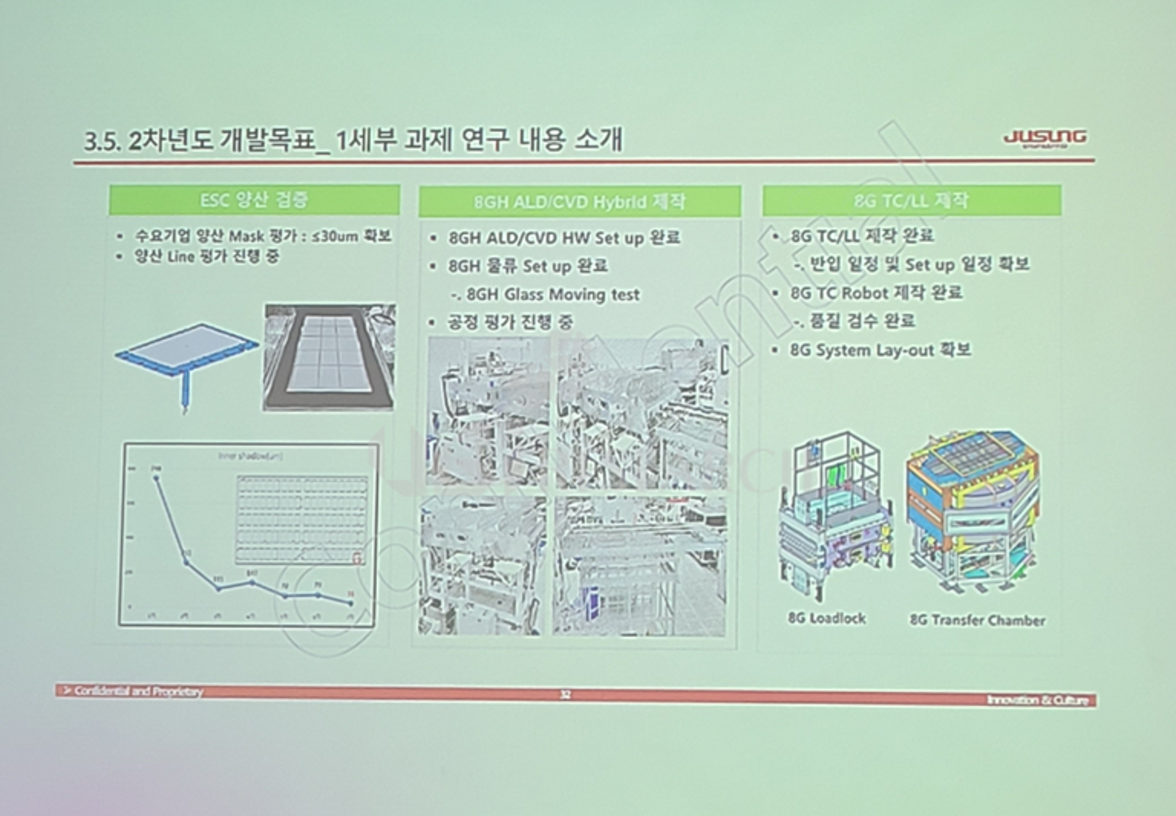
In the second year, 2022, low-hydrogen composite membrane evaluation for 8th-generation half equipment is underway. Unit process evaluation using 6G half and 8G half equipment is scheduled for evaluation in November, and the details of the first detail task research in the second year include ESC mass production verification, 8G half ALC/CVD Hybrid production, and 8G TC/LL production.

Lastly, they concluded presentation by emphasizing that “The expected effect of the research project is to strengthen the global competitiveness of materials-parts-equipment companies and to secure source technologies, and major domestic companies also have the advantage of reducing their dependence on foreign equipment and improving their development speed. On a national level, it can be a good opportunity not only to stabilize employment and create jobs, but also to transform from an importing country of materials, parts, and equipment to an exporting country.”

[China Trend Report] Visionox Orders 6th Generation Vertical Vapor Deposition for IT

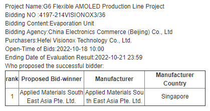
According to a Chinese trend report published twice a month by UBI Research, Visionox ordered sixth-generation vertical vapor deposition machines for R&D on the V3 line.

Visionox Ordered Vertical Vapor Deposition, Source: Chinabidding.com

Visionox Ordered Vertical Vapor Deposition, Source: Chinabidding.com

Visionox’s V3 line is operated on with 30K/Month to mass-produce flexible OLEDs and this investment was done mainly on deposition process equipment in the spare space of the V3 site without investing in cells or module process equipment for IT.

The 6th generation vertical vapor deposition machine invested by Visionox this time is considered to be a prior investment to secure the technology of vertical vapor deposition and to determine the possibility of mass production in the 8th generation or higher in the future. The deposition process in the existing OLED line is being carried out as a horizontal deposition process and due to the issue of ledger glass and FMM control, FMM technology is applied to half-cut in the 6th generation line for mobile devices and open-mask technology in the 8th generation line for TV.

Since glass and masks are less affected by gravity than horizontal deposition, vertical deposition has the advantage of securing greater productivity by allowing deposition without cutting the ledger glass. However, mass production is still unclear.

If Visionox secures technology for vertical deposition through this investment, it is expected to invest in new lines for 8.5th generation IT without half-cut in the future.

▶ China Trend Report Inquiry
JDI decided to sell LCD production equipment to a foreign client for 200 million dollars

JDI announced that it has agreed to sell production equipment at its plant in Hakusan, Ishikawa Prefecture, to a foreign client for 200 million dollars.

The Hakusan plant was JDI’s mainstay factory, producing LCD panels for Apple. The plant was halted in July last year due to sluggish demand. JDI plans to clean up excess facilities that have caused poor performance.

JDI decided to sell LCD production equipment to Apple first and real estate to Sharp later, but negotiations have been delayed due to the effect of the corona virus.

The Hakusan plant was built with Apple’s $ 1.5 billion funds and operated at the end of 2016. But because Apple’s utilization of OLED panels on iPhones has increased in recent years, utilization rate of Hakusan plant has decreased. Moreover, it was a burden for JDI to repay the advances to Apple at the end of February 2020. It is a policy that the funds obtained through the sale of the equipment will be used to repay advances.

Wuhan Tianma 6G OLED line installation delay

The Tianma T4 plant in Wuhan has continued to produce even during the corona period, and the core equipment of the ph2 6G OLED line has already been brought in, but the equipment set-up is delayed due to the inability of overseas equipment companies to enter Wuhan.

In recent, as the number of corona virus spreaders in China, including Wuhan, has declined, equipment set-up is expected to resume from the second quarter, and mass production is expected to start after the third quarter.

The ph2 of Tianma T4 was signed on June 1, 2018, and a total of RMB 14.5 billion was invested. When the Ph2 setup is complete, the Tianma T4 plant will have a total of 35K Capa in 6G.

2020 OLED Manufacturing Equipment Market Forecast

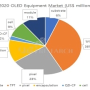
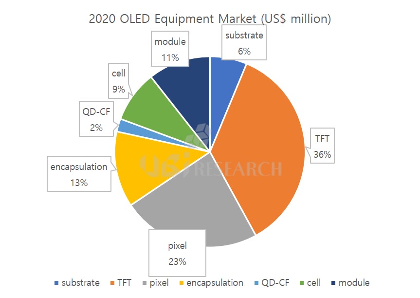
According to UBI Research’s annual equipment market track for 2020, the OLED manufacturing equipment market is expected to reach $ 9.51 billion in 2020. This is an increase of $ 1.2 billion compared to $ 8.31 billion in 2019.

Chinese panel makers have aggressively invested the 6G Flexible OLED line, but due to the high panel price, the adoption of flexible OLED produced in China in the smartphone market has not increased, leading to an oversupply of over 30% worldwide. For this reason, Korea has stopped investing in 6G flexible OLED, and Chinese panel makers are also delaying their investment time slightly.

However, by 2020, Samsung Display’s investment in the 8.5G QD-OLED 30K line began, and the equipment market will remain at the 2019 level.

AP System supplies ELA equipment to Chongqing BOE B12

AP System was selected as the final bidder for BOE’s B12 line ELA (eximer laser annealing) equipment.

ELA is an essential equipment to make low temperature polysilicon (LTPS) TFT for OLED. Eximer laser crystallizes a-Si into polysilicon. It is called LTPS because it makes polysilicon without applying high heat.

In this bid, BOE presented not only equipment quality but also technical competitiveness, easy operation, and maintenance as a supply condition. The AP system met all these requirements and became a final equipment supplier. The official PO has not come out yet.

BOE B12 plans to install eight ELA units. AP System also supplied ELA equipment to BOE’s B7 and B11.

Samsung Display decided to invest 13 trillion won in QD-OLED by 2025

Samsung Display chose QD-OLED as the next generation premium TV. It will also have a big impact on the premium TV market, which is divided between white OLED technology and QLED technology.

Samsung Display announced a new investment and win-win cooperation agreement ceremony at Asan Campus on October 10 and will invest a total of KRW 13 trillion in QD-OLED production facilities and R & D by 2025.

The basic structure of QD-OLED is composed of blue OLED and red and green quantum dot color filters (QD-CF). Blue OLEDs emit blue light, and the red and green QD-CFs convert them to red and green, respectively. QD is also applied to QLEDs because it has the effect of further improving color purity.

Samsung Display will invest 13 trillion won by 2025 to build the world’s first QD display mass production line ‘Q1 Line’ at Asan Campus. The new line will start production in full scale in 2021 with an initial 30,000 sheets (8.5 generations) and will produce a 65-inch or larger ultra-large QD display. To this end, the company plans to convert existing 8G LCD lines into QD OLED lines step by step and gradually expand production capacity by 2025.

In addition, in order to accelerate the commercialization of new QD technology, the company plans to shift the existing LCD workforce to QD and hire new QD materials and process development experts. Samsung Display predicted that if investments start in earnest, approximately 81,000 jobs will be created over the next five years.

Lee Dong-hoon, president of Samsung Display, emphasized that “QD, a semiconductor particle that emits light close to natural colors, is the future growth vision of the large display industry.” “We will lead the premium display market with this investment.”

[Press Release] OLED production capacity will increase to double in 2023.

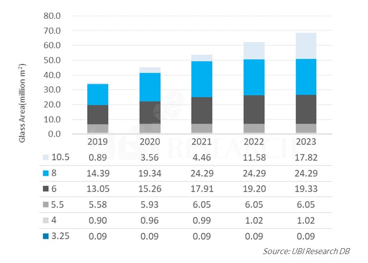
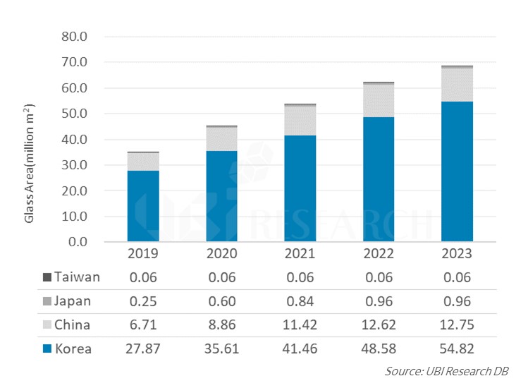
UBI Research has published [2019 OLED Equipment Report] that forecasts the OLED equipment market. According to the report, the total substrate area of display companies in 2019 will be 34.9 million square meters, which will be 68.5 million square meters in 2023 and double after four years.

OLED substrate area growth is attributable to investments made by OLED lines for TVs driven by Samsung Display and LG Display. Currently, OLED manufacturing lines for TVs are 8G lines optimized for 55-inch panel production. However, the demand for premium TVs is shifting from 55-inch OLED TVs to 65-inch TVs. By 2021, the 65-inch OLED TV market will account for more than 40%. In response to these market conditions, LG Display is preparing to invest 10.5G lines in the most efficient production of 65-inch panels. In 2023, the substrate area of a large OLED line is expected to occupy 42% of the total substrate area.

<OLED production capacity by generation>

The substrate area of the 6G line is expected to grow to 13 million square meters this year and to 19.3 million square meters in 2023. Most of this is due to investment by Chinese panel makers. In China, the smartphone market accounts for about 40% of the global market, so Chinese smartphone makers have a very high market share based on the domestic market. Huawei has recently become the world’s second-largest shipper based on its domestic market. Chinese panel makers are boldly adding a 6G flexible OLED line to Chinese smartphone makers, with the Chinese government’s huge support.

<OLED production capacity by country>

In 2019, Korea’s OLED production capacity (substrate area) will total 27.9 million square meters, accounting for 80% of its total production capacity and expanding to 54.8 million square meters by 2023. The market share will remain at 80% and lead the OLED industry.

Chinese panel makers are expected to stay at around 20% as they are investing only in OLED production lines for mobile device.

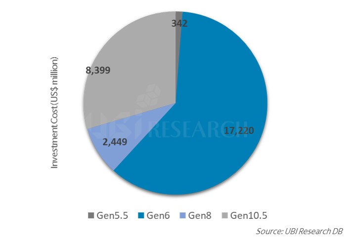
The OLED manufacturing equipment market (excluding logistics equipment) is estimated at $ 28.4 billion for four years from 2019 to 2022 due to investment by Korean and Chinese panel makers. Among them, the sixth-generation equipment market is expected to account for 61% of the total equipment market, at $ 17.2 billion.

<Equipment Market Forecast by Generation (2019 ~ 2022)>

2019 Chinese OLED panel maker equipment order status

As Korean OLED panel makers do not have a lot of investment, the OLED equipment industry is in a low-demand season. When Chinese OLED panel makers confirm the order status of equipment orders in 2019, orders are being made centering on equipment and module line equipment required for new technologies rather than new lines.

In China panel makers BOE and CSOT, some equipment was ordered in March of this year for the development of flexible on-cell touch technology, and Korean equipment makers seem to have received orders from Wonik IPS and Iruja. In addition, since last month, the BOE Chengdu line has begun full-scale mass production and ordering of modular products along with foldable product preparation. Korean equipment makers will also receive equipment orders from BOE and proceed with production.

Starting this month, Visionox Hebei Line, which is set to start full-fledged investment this year, has begun placing orders for long-term delivery equipment and automation equipment. In addition, Wuhan Tianma is making some complementary investments in flexible process equipment, and EDO, Royole, and Truly are expected to invest in the future depending on market conditions.

UBI Research AMOLED process equipment industry report, which is scheduled to be published in May 2019, will be covered in detail in investment situation and equipment supply chain in China panel makers.

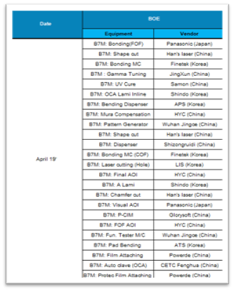
[BOE Chengdu Module Line Order Status]

OLEDON, is to announce belt-plane source deposition technology for manufacturing ultra-high resolution and ultra-area OLED

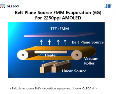
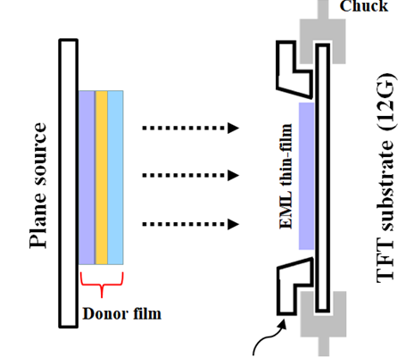
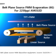
Plane source technology, which was first developed by OLEDON in the world, has the principle of depositing the first organic material on the metal surface and evaporating it upwards to produce fine pattern of 2250 ppi, which is ultrahigh resolution. In this plane source process, three processes such as the first deposition, the plane source inversion, and the second evaporation are necessary, and the number of the high vacuum chambers is increased when the mass production is applied. The belt plane source FMM deposition technology introduced by OLEDON has a concept of carrying out the above processes at a time in one evaporation equipment. This is a continuous plane source supplying deposition technology in which the metal surface is formed in a belt shape.

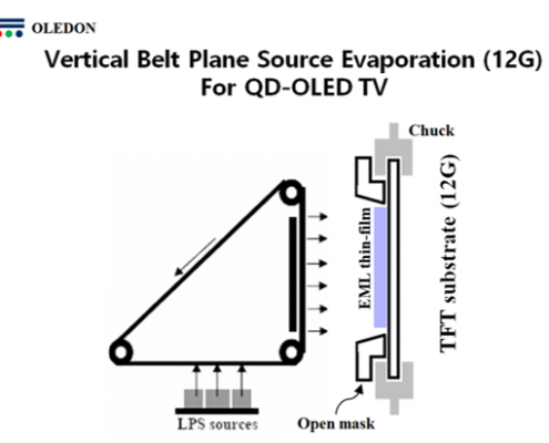
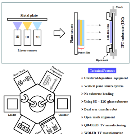
Hwang added, “Using vertical plane source enables smooth deposition process for the 12th generation class area substrate for QD-OLED TV without sagging problem. Vertical belt-plane source evaporation equipment adopts the concept of depositing the substrate in a standing-up position so that the load on the framed glass chuck and the open mask is very low. Thus, easy transportation of the substrate, and uniform deposition process of thin film over a very large area in the static state are possible.” This technology is expected to be applicable not only to the 8th generation but also to the cluster type mass-production evaporator with substrate sizes more than 10 generations in the future.

<Vertical belt plane source evaporator for QD-OLED, Source: OLEDON>

Commenting finally that the company has successfully completed the material denaturation test for blue materials and the blue dopant deposition test, Hwang expected the plane source deposition technology to be applied to both small & medium sized OLED and large area OLED manufacturing in future.

On the other hand, OLEDON holds more than 30 related patents including original patents of plane source and belt plane source evaporator. Also, the company recently filed a patent related to a vertical belt plane source evaporator for mass production.


OLEDON unveils plane source deposition technology for ‘super-gap’ OLED manufacturing.

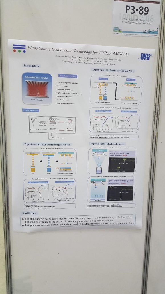
Attention is growing since OLEDON, a venture company developing OLED deposition equipment, unveiled plane source deposition technology for OLED manufacturing to maintain ‘a superb gap with the competing countries’, at IMID2018, held in COEX, Seoul, Oct. 24, 2018.

Hwang Chang-Hoon, CEO of OLEDON, said, “Korea should actively invest in the development of creative deposition technology to maintain the first place in the current OLED producing countries.” He expects that plane source deposition technology is to be used both for small and medium size OLED and large area OLED manufacturing in future.
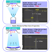
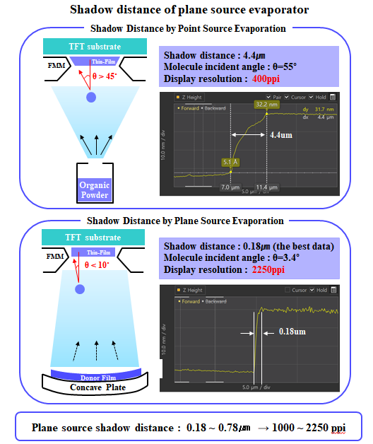
OLEDON is developing the world’s first curved plane source FMM deposition technology, which is an ultra-high-resolution OLED deposition technology capable of manufacturing 2250ppi AMOLED. The shadow distance of fine pattern can be up to 0.18um, enabling 11K high-resolution AMOLED pattern process.

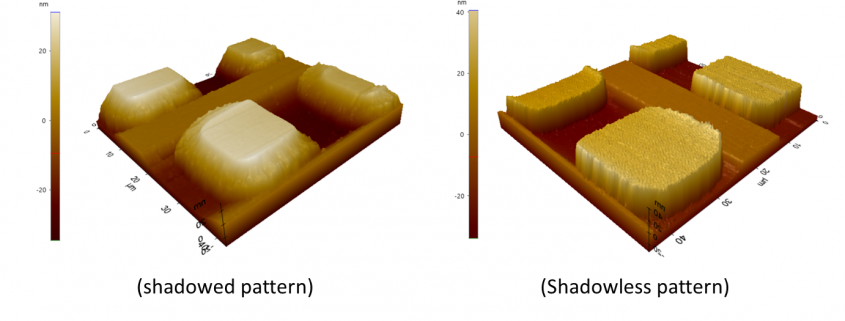
<Existing FMM deposition pattern (left) and plane source FMM deposition pattern (right), Source: OLEDON>

According to Hwang, this process was confirmed with 800 ppi shadow mask, and the emission area of the pattern deposited with plane source was 1.7 times higher than the conventional deposition method.
On the other hand, OLEDON holds the original patent for the FMM deposition technology of plane source, and has recently applied for a patent for vertical plane source deposition for large area OLED TV manufacturing.

<Vertical plane source deposition for OLED TV manufacturing, Source: OLEDON>

OLEDON develops vertical plane source deposition technology for large OLED TV manufacturing

Hwang Chang-Hoon, CEO of OLEDON, which has developed plane-source deposition technology for small & medium-sized OLED and large area OLED, said that it is under development of vertical plane source deposition technology capable of manufacturing ultra-large OLED TVs of 77 inches or larger. Hwang introduced the related technology that it is possible to mass produce OLED TVs of 77 inches or more without the sagging problem of large substrate such as 12th generation (3300 x 4000 mm) substrate when using vertical plane source deposition technology.

According to Hwang, the production yield for 75 inch TVs or larger with the conventional inline type evaporator might be very low due to severe sagging of the substrate and difficult control of many linear sources. To solve this problem, Hwang said that a new 12-generation large-area cluster-type deposition technology is needed, and that vertical plane source deposition technology will be an appropriate alternative.

On the other hand, OLEDON holds the original patents for plane source deposition technology. It also filed a patent related to the curved plane source FMM deposition for high-resolution AMOLED manufacturing, and a patent related to the vertical plane source deposition technology for manufacturing large-area OLED TV.


[IMID 2018] OLEDON, developed ‘curved plane source FMM deposition technology’ for 2250ppi AMOLED for the first time in the world

OLEDON is a company which develops plane source deposition technology for high resolution AMOLED manufacturing. Hwang Chang-Hoon, CEO of  OLEDON announced in IMID 2018 that it developed ‘curved plane source FMM deposition technology’ that can be adopted to 2250ppi AMOLED pixels, for the first time in the world.

Conventional linear source FMM deposition technology has a shadow distance of 3um. The available production range is 570ppi AMOLED resolution. On the other hand, the plane source deposition technology already demonstrated in OLEDON can achieve a resolution of 800 to 1200 ppi of AMOLED with a shadow distance of 0.8 to 1.5 μm. Meanwhile, the newly developed ‘curved plane source FMM deposition technology’ is an upgraded technology of the plane source deposition technology which can realize the maximum resolution of AMOLED to 2250ppi with a shadow distance of 0.18 ~ 0.6μm.

The principle is that light is gathered through a concave mirror, a curved surface is applied to the conventional flat plane source, and the light emitting material does not spread, but is precisely deposited at a desired position, thereby reducing the shadow distance.

If this technology is commercialized, it is expected that it can be widely applied not only to mobile devices but also to virtual reality devices.

How much will be the investment cost for 8Generation QD-OLED TV?

In the “2018 OLED Equipment Report” recently published by UBI Research, the required investment cost was analyzed for the QD-OLED that Samsung Display started to develop.

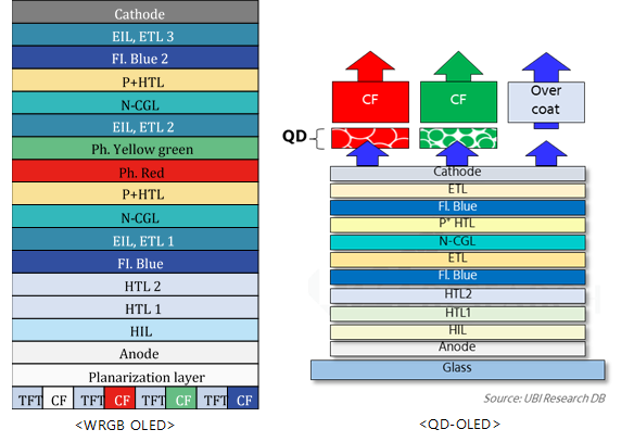
QD-OLED, which is being developed by Samsung Display, is a method of displaying three colors of RGB by separating green and red from the light emitted from blue OLED through QD (quantum dot) material. The light passing through the QD material once again passes through the color filter and displays a richer color.

QD-OLED is similar to the manufacturing method of WDRGB OLED produced by LG Display. First, both companies use oxide TFTs. At WRGB OLED, blue is applied twice and red and green are deposited between them. In contrast, QD-OLED is fabricated by depositing only blue material twice. Both methods use the open mask with an empty center.

For both QD-OLED and WRGB OLED, the color filter manufacturing cost is assumed to be same; however, QD-OLED should be equipped with additional equipment to coat QD materials.

According to the report, it is expected that the investment cost is to be equal because the similar equipment can be used for module, cell, encapsulation and evaporator. Since WRGB OLED is bottom emission type, it is formed together when backplane is formed including TFT. However, QD-OLED adopts top emission method. A color filter is separately formed on the top glass substrate and the QD layer is patterned thereon. Therefore, QD-OLED requires higher investment cost than WRGB OLED.

The report describes that based on 8Generation 26K, the investment cost for QD-OLED is estimated to be US$ 1.1 billion, which is 1.03 times higher than WRGB OLED (US$ 1.07 billion). In contrast, the required investment cost to manufacture OLED by inkjet method, which JOLED is promoting commercialization, is projected as US$ 0.88 billion, which is to be about 80% of QD-OLED.

[iMiD 2017] OLEDON, Disclose plane source FMM deposition principle for 2250ppi OLED manufacturing

Prof. Hwang Chang-Hoon, CEO of OLEDON, a venture laboratory of Dankook University, presented a plane source FMM deposition technology capable of implementing 2250 ppi at iMiD 2017 held on the 28th.

According to Prof. Hwang Chang-Hoon’s presentation, the plane source deposition technology developed by OLEDON differs from the existing organic material deposition method. The plane source FMM deposition technique is that the organic material is first deposited on the metal surface to form a donor film and then re-evaporate it to form an organic thin film on the substrate. Applying this technique, organic matter forms a vertical gas beam due to plane evaporation. (Source patent: 1012061620000 Republic of Korea)

The shadow distance when organics are deposited with a plane source developed by OLEDON is 0.38 μm – 0.59 μm. This is a level at which a 2250ppi device having a pattern size of 4 um can be manufactured.

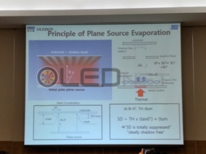
Prof. Hwang Chang-Hoon explained ‘applying the plane source deposition technique reduces the incidence angle of the organic material and dramatically reduces the shadow caused by the mask’. In addition, ‘using a plane source, the perpendicular organic gas beam can form a completely zero incident angle, so theoretically, the shadow distance can be zero um’.

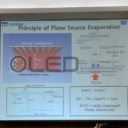
<Principle of plane source deposition technology developed by OLEDON>

In addition, Prof. Hwang Chang-Hoon emphasized that ‘plane source deposition technology is essential for high-resolution shadow masks’.

For linear source FMMs currently in production, the shadow mask opening distance is 80 μm. As a result, the incidence angle of the organic material gas is inevitably large, making it difficult to produce a shadow mask having a high density pattern.

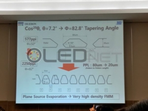
Prof. Hwang Chang-Hoon explained, ‘Using plane source deposition technology, shadow mask taping angle is 80 ° level’, and the distance between openings can be reduced to less than 20 μm so that plane source deposition techniques can solve the mask pattern density problems of linear sources’.

OLEDON is challenging fully shadow-free patterning conditions with plane source deposition technology, and plan to develop and install a plane source FMM evaporator capable of manufacturing 11K class micro OLED devices in cooperation with Prof. Jin Byung-Doo in Dankook University. (Reference: Homepage of OLEDON www.oledon.co.kr)

<The opening density change of the shadow mask when the plane source FMM deposition technique is used>

Meanwhile, OLEDON has 13 registered patents for plane source FMM deposition for mass production. Based on recent research results, they filed 7 new patents for mass production equipment in Korea and 3 applications are filed for PCT international application.